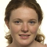
People
Professor William (Bill) Milne
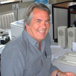
Research interests include large area metal oxide and carbon based electronics, thin film materials and, most recently, MEMS, carbon nanotubes and other low-dimensional structures for electronic applications. Current projects include optimization of CNTs and graphene for field emission applications especially for portable x-ray systems. Other main interest at present is in the use of an SOI platform for Gas sensing application in collaboration with a start-up company Cambridge CMOS Sensors [founders, Florin Udrea, Bill Milne and Julian Gardner (Warwick University)].
The use of Graphene for high frequency applications is also being carried out where a major push is towards application in the terahertz range.
Professor John Robertson

Research interests include: Carbon Nanotubes, graphene, chemical vapour deposition, electronic applications (experimental and calculation). Modelling of CVD mechanisms. Carbon interconnects, carbon conductors, carbon for supercapacitors. High dielectric constant (K) oxides for complementary metal oxide semiconductor transistors. High K oxides on high mobility substrates such as InGaAs, Ge (modelling). Transparent conducting oxides, amorphous oxide semiconductors (AOS) such as InGaZn oxide, their thin film transistors, instability mechanisms (calculations). Density functional calculations of semiconductors, oxides, carbon materials, and hybrid density functional calculations for correct band gaps. Functional oxides, TiO2.
Professor Michael J Kelly
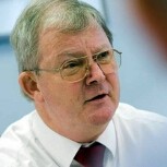
Professor Kelly's research aims to answer the following questions: Most of today’s nanoscience will never become a nanotechnology, not least because of the inability to control intrinsic fluctuations in small structures. What subset of nanostructures is manufacturable in practice? Electron tunneling devices make extreme demands on interface integrity, with special growth techniques needed to achieve tunnel devices. How can these techniques be achieved? What practical devices might emerge from exploiting the quantum coherence of electrons as waves in semiconductors: the quantum multiplexer? Any serious reduction in carbon dioxide emissions requires the whole scale retrofit of the national building stock? How practicable is this? How is scientific uncertainty to be cast and acknowledged in the formation of national policies on energy, buildings etc, with special reference to climate science?
Professor Andrew Flewitt
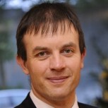
In recent years, metal oxides have emerged as a viable alternative to amorphous silicon in thin film transistors for display applications. This is due to their significantly higher carrier mobility and potentially improved stability. Furthermore, these materials are more suited to plastic substrates, and so open up a range of new plastic electronics applications. Our work in this field, much of which has been performed through the Cambridge Integrated Knowledge Centre, has focussed on two general themes. The first is manufacturability. Magnetron sputtering, which is most commonly used to deposit these materials, suffers from problems in terms of reproducibility and scale-up. We have been investigating the use of other deposition technologies, including a High Target Utilisation (HiTUS) sputtering system, which are more suited to scale-up. Using the HiTUS system we have demonstrated a new phase of amorphous hafnium oxide - cubic-like amorphous hafnium oxide (ca-HfOx) - which has a fully amorphous structure and a dielectric constant of over 30, and is a significant improvement over the state-of-the-art. These materials have been incorporated into a variety of devices.
Our work on acoustic wave sensors is based on both surface acoustic wave (SAW) devices and film bulk acoustic resonator (FBAR) devices. In both cases, we most commonly use zinc oxide that is sputtered with a very low stress (<100 MPa) using our HiTUS sputtering system (see above). This has allowed us to produce FABR devices with operating frequencies between 1 and 2 GHz and with a Q-factor of ~1500. These devices are being developed mainly for biosensing applications.
We have also started to use our metal oxide materials for solar cells. In particular, we can produce a high mobility cuprous oxide, which is p-type and has a Hall mobility of ~10 cm2 V-1 s-1. Cuprous oxide has a band gap ~2 eV, and so is ideal for the absorber layer in solar cells.
We also work on zinc oxide nanowires for tactile surfaces. This again uses the piezoelectric properties of zinc oxide to both detect deflection and produce deflection. We use thin films of nanowires to make touch-sensitive surfaces for future generations of touch-sensitive displays and surfaces.
Please visit Dr Flewitt's home page for further details.
Professor Stephan Hofmann
Dr Hofmann’s research explores novel materials, metrology and device architectures. A particular focus thereby lies on nanomaterials, such as graphene, carbon nanotubes and semiconductor nanowires, and the use of in-situ metrology to probe the fundamental mechanisms that govern their growth and functionality.
The nanometer dimensions can lead to extraordinary properties and being able to control and exploit those can have a transformative impact across a wide range of applications, such as information/communication technologies, energy generation, conversion and storage, and environmental and bio-technology. The vision of Dr Hofmann’s research is to unlock this huge technological potential through an unprecedented understanding of material design and functionality on the smallest of size scales.
Dr Hofmann is leading a number of large research projects, funded eg by the ERC and EPSRC, with close industrial links and embedded in a large network of international collaborations.
Please visit Dr Hofmann’s research group homepage for further details.
Dr Hannah Joyce
