

University of Cambridge
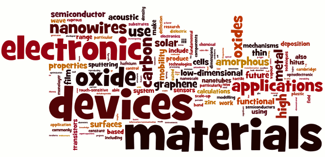
The Electronic Devices & Materials (EDM) Group's research includes topics that range from the nanometre scale through individual devices to large area electronics. It covers a diverse range incorporating development of micro-and nano-electro mechanical structures (MEMS and NEMS) and sensors with applications in biotechnology and optics. Work is also aimed at the investigation of various backplane technologies including a-Si and more recently Metal Oxides including ZnO and IGZO. A major effort is on the growth, characterisation and application of a range of nanomaterials including Semiconducting Nanowires (Si, Ge, III-V, Zinc Oxide), Carbon Nanotubes, Graphene and other 2D materials.
Web Design by:jpn25