
Facilities
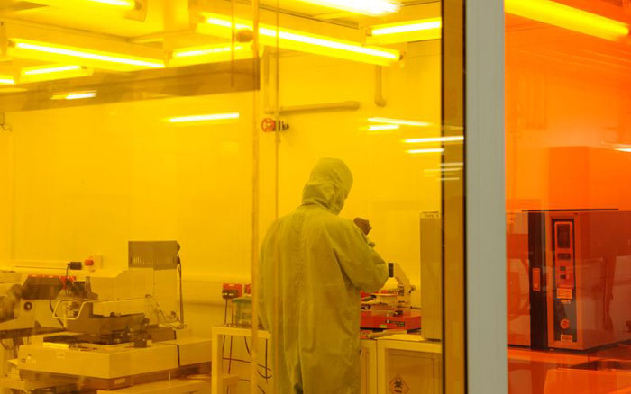
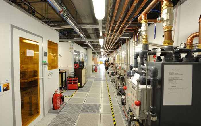
The University of Cambridge Electrical Engineering Division building opened in 2006 and houses custom-built state-of-the-art photonics and electronics research and prototype development facilities across approx. 5,000m2 of lab space, including class 100 (140 m2), class 1000 (140 m2) and class 10k (160 m2) clean room facilities.
The Engineering Clean Facility is available to be used by academic and industry users. If you are interested in accessing the Facility, please contact Dr Andrew Flewitt, who will be able to provide up to date information regarding access charges and training.
Available equipment includes:
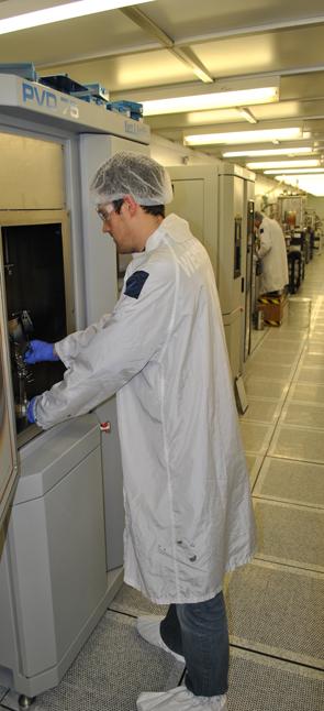
Specialist deposition systems:
 Cold- and hot-walled, thermal and plasma enhanced CVD reactors for the growth of graphene and carbon nanotubes (9 different reactors ranging from high vacuum to atmospheric pressure)
Cold- and hot-walled CVD reactors for the growth of semiconducting nanowires
ECWR plasma and Filtered Cathodic Arc deposition systems for the deposition of amorphous carbon films
Thermal and plasma enhanced CVD reactors for the deposition of amorphous Si thin films
Plasma enhanced and thermal Atomic Layer Deposition (ALD) reactors
Remote plasma and ion beam sputterer for the deposition of functional oxide thin films
Thermal and e-beam evaporators
Magnetron, RF and DC sputterers
Device processing facilities:
Optical Mask Aligners
(0.5µm with 2µm front-to-backside alignment)
E-beam Lithography
Reactive Ion etching (RIE and DRIE) systems
Acid and Solvent Bays
Annealing and oxidation furnaces
Wire and Device bonders
Inkjet Printer
Ultra-centrifuges and Sonicators
Langmuir-Blodgett equipment