Sir Charles Oatley and the Scanning Electron Microscope
Research Post Stereoscan
II. RESEARCH
DIRECTED BY W. C. NIXON
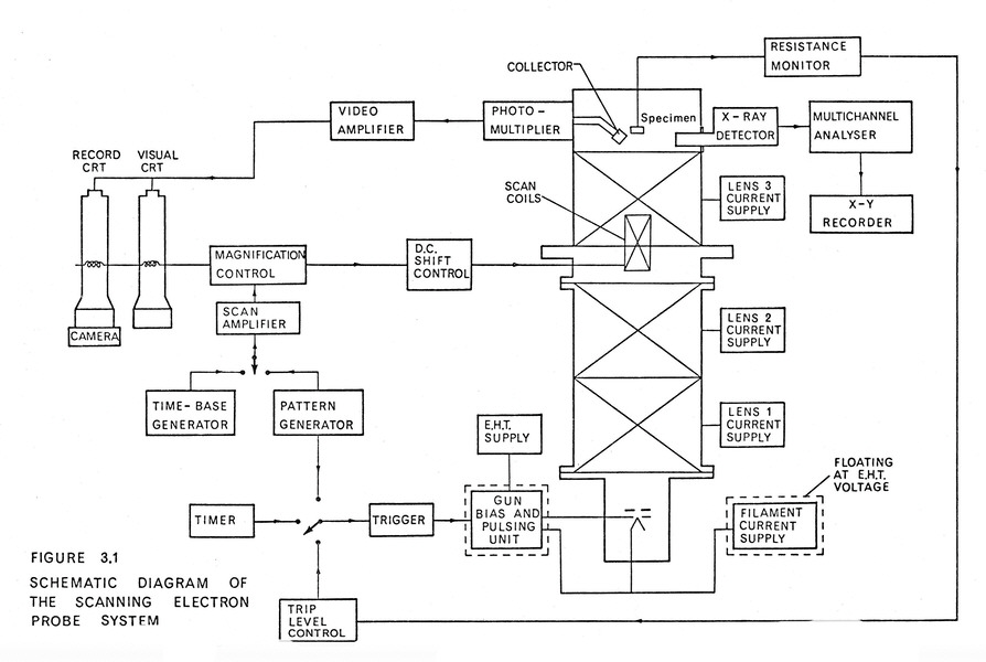
Contributed by K. C. A. Smith and B. C. Breton 
A. Novel electron optical systems
Bill Nixon's appointment as Assistant Director of Research in the Engineering Department in 1959 came at a critical time when the prospects for the SEM were still uncertain. The crucial role he played shortly after his appointment in the negotiations leading to the commercial development of the SEM at CIC is describedin Volume 133, Chapter 4.1A. Their successful outcome provided a firm foundation on which the programme of research on the SEM in the Department could be continued and expanded.
The period between 1960 and 1965 were years of transition during which Oatley’s attention was increasingly engaged with reform of the teaching of electronics and with other duties associated with his appointment to the Chair of Electrical Engineering, while the time he was able to devote to research rapidly diminished. During this period Nixon took over the direction of the research, including the supervision of Oatley’s existing research students.
The work of the first of these students, Pease and Broers, is described in Chapters 2.9A and 2.10 of Volume 133. They commenced their PhD work under Oatley, in 1960 and 1961 respectively, but then became the responsibility of Nixon, Pease after one year and Broers after one term of research.
Gary Stewart, who started his research in 1958 under Oatley, was another student whom Nixon advised, and it was he who was instrumental in steering Stewart towards taking employment with CIC. Nixon took over Oatley’s last student, Philip Chang, in 1964 when he had completed one year of research. An account of Chang’s work in connection with electron beam lithography is given by Bernard Wallman in Chapter 4.4 of Volume 133.
With the launch of the Stereoscan the SEM had, as Oatley put it, “come of age”, and it fell to Nixon to consolidate much of what had gone before in the Department and to take the initiative in exploring new avenues of research in electron optics.
A. Novel Electron Optical Systems
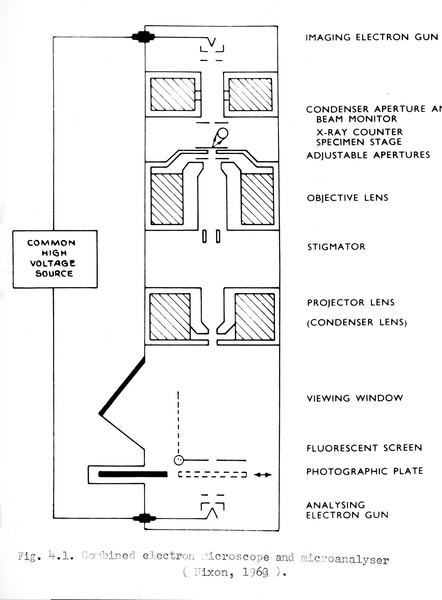
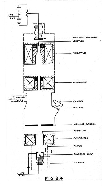
While still in Cosslett’s Group at the Cavendish Nixon had conceived a novel method of combined microscopy and x-ray microanalysis. The implementation of this idea fell to his first student in the Engineering Department, Bob Buchanan, who commenced his PhD research in 1960. The essentials of Nixon’s scheme are shown in [Buchanan, Fig. 4.1] of Buchanan’s dissertation (Buchanan, 1964). To a normal transmission electron microscope is added a second electron gun - the analysing gun - mounted below the fluorescent screen. Both guns in the system share a common HT supply. A hole in the screen allows the beam from the analysing gun to pass in the reverse direction through the column forming a demagnified image of the gun crossover in the plane of the specimen. The fine electron probe thus produced strikes the specimen in an area delineated by the hole in the fluorescent screen.
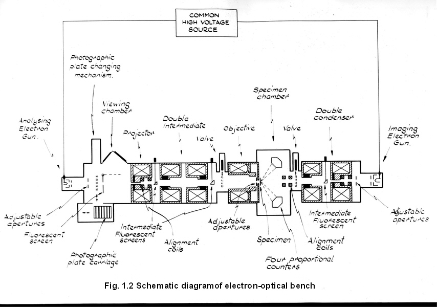
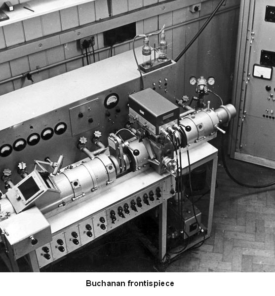
Buchanan's implementation of this scheme is shown in [Buchanan, Fig. 1.2]. The imaging system consists of a normal transmission microscope with double condenser, objective lens, and three-stage projector. The probe forming system comprises the analysing gun, the projector lenses and the objective lens. The whole is arranged in the form of a horizontal electron optical bench, with the guns at its extreme ends. A photograph of the complete apparatus is shown in [Buchanan, Frontispiece].
Although in principle the focal conditions for both imaging and probe forming are the same, because of the Earth's magnetic field and other factors there is some displacement between the probe and the area corresponding to the hole in the fluorescent screen. For this reason it was found it necessary to incorporate alignment coils within the column, and to devise a procedure to correct pap for this displacement. Special procedures were also devised for correcting astigmatism. In the course on the work some interesting and novel aspects of the interaction between the electron probe and supporting films were investigated.
The X-ray analysis equipment comprised four gas-flow proportional counters with their associated counting and pulse height analysis of electronics. Four counters were used, connected in series, to increase the collection efficiency. [Buchanan, Fig. 5.2] shows the measured efficiency of the four-counter array. Because of the high intensity of background radiation due to X rays generated by electron scattering within the specimen chamber microanalysis was not successful. Means for overcoming this difficulty were suggested. This experimental works was complemented by a theoretical treatment of x-ray microanalysis of thin films in which expressions were evolved for both the characteristic and continuous x-ray emission intensities.
The topic given in 1962 to another of Nixon’s students, Mike Barnett, also represented something of a departure from the programme of research hitherto conducted in the Department. This concerned a theoretical and experimental investigation of mirror electron microscopy, a technique that had its origins in Germany in the years leading up to World War II.
To gain experience with the method Barnett constructed first a two-lens and then a three-lens column, largely out of surplus components available in the laboratory. With these he was able to obtain some interesting mirror images of a variety of specimens including magnetic domains on a cobalt crystal. [Barnett, Plate. 2.4] (Barnett 1966) is a schematic diagram of the three-lens column, and [Barnett, Plate. 2.1] is an example of a magnetic domain structure.
This experimental work was complemented by an extended theoretical discussion concerning the properties of the electrostatic electron mirror in the course of which Barnett points to a number of errors and invalid assumptions made in the publications of previous authors. An important aspect of the theoretical discussion was an elucidation of the electrical and magnetic contrast mechanisms arising in the mirror microscope. He also discusses the resolution to be expected and shows that the wave mechanical approach used in earlier work is inadequate to explain the limits to resolution, and argues that several factors are involved including the effect of thermal velocities.
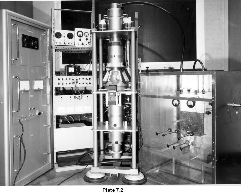
The preliminary experimental work coupled with the theoretical development of the subject provided a foundation for the design of a new electron optical column, shown schematically in [Barnett, Plate. 7.1]. [Barnett, Plate. 7.2] is a photograph of the completed instrument. It contained five magnetic lenses - two condensers two projectors and an objective – and incorporated the necessary facilities for alignment and control of the complex imaging modes possible with mirror operation. The design also took into account the possibility of adapting the instrument for emission or scanning microscopy. (Dr John Garrood later added scanning to the column, but as far as can be ascertained no account of his work exists.)
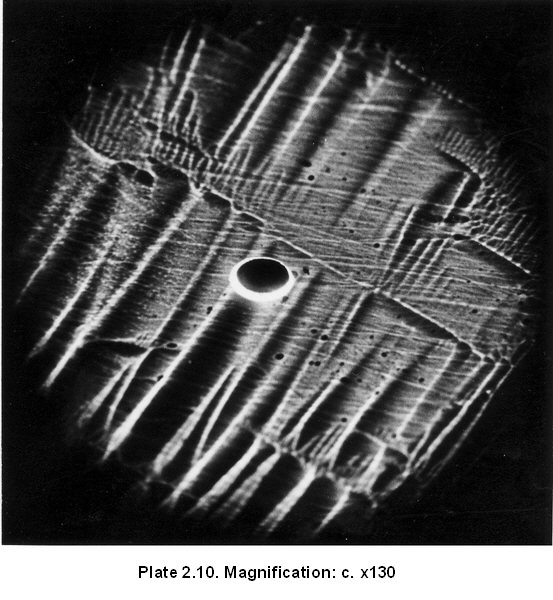
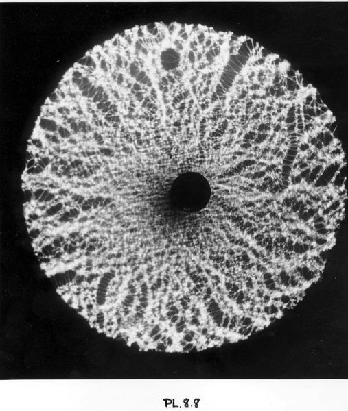
In his dissertation Barnett presents a large selection of mirror images obtained with the new column, the interpretation of which in many instances required recourse to the theory develop earlier. One of the most successful applications of the technique was to the observation of magnetic domain structure, which up to that time the SEM had failed to reveal (but see Banbury below). [Barnett, Plate. 8.8] shows the contrast obtained from the hexagonal face of the same cobalt crystal as used to obtain [Barnett, Plate. 2.1]. Barnett likens the contrast in this micrograph to the classic ‘lace-patterns’ observed when using the Bitter powder pattern technique. The pattern recorded on magnetic audio tape was also revealed successfully.
After completing his research in the Department, Barnett took up an appointment at Imperial College, London, where he collaborated with Otto Klemperer in the production of the Third Edition of Klemperer's book on the electron optics (Klemperer and Barnett, 1971).
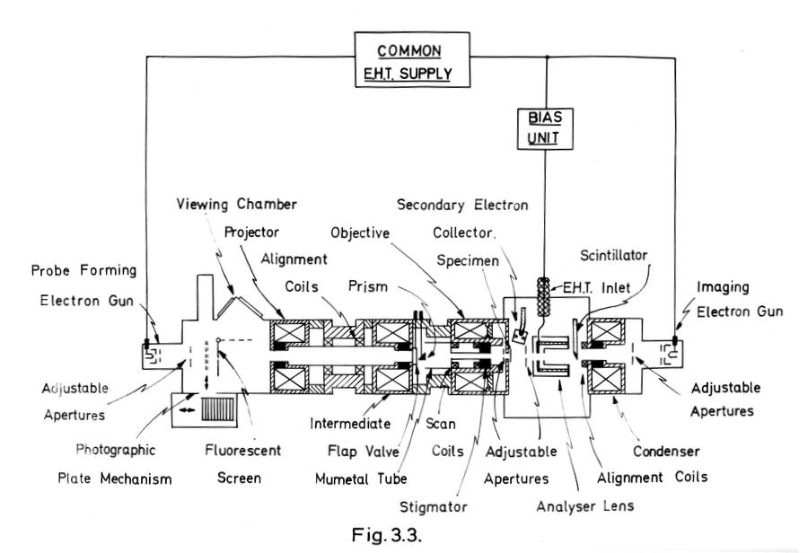
Nixon’s next student, Dick Paden, who commenced his PhD project in 1963, continued work on the electron optical bench started by Barnett, but x-ray microanalysis was discontinued in favour of the more promising approach offered by electron energy loss analysis. To this end an electron energy analysis system was added to the column, the main component of which was a transmission ‘einzel’ filter lens. The use of this type of filter lens had the advantage that, by offering a free path along its axis, normal operation of the electron optical bench as a transmission instrument could be retained. The filter lens was accommodated in a new, enlarged specimen chamber, which incorporated also facilities for scanning reflection and scanning transmission operation. A cross-sectional diagram of the revised layout, with additional features incorporated by Paden, is shown in [Paden, Fig. 3.30] (Paden, 1964). This should be compared with Buchanan's, Fig. 1.2.
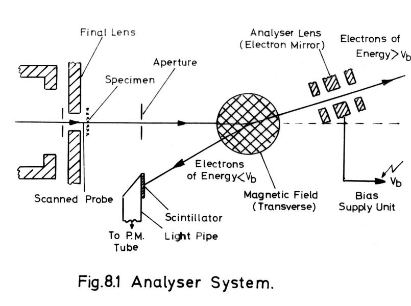
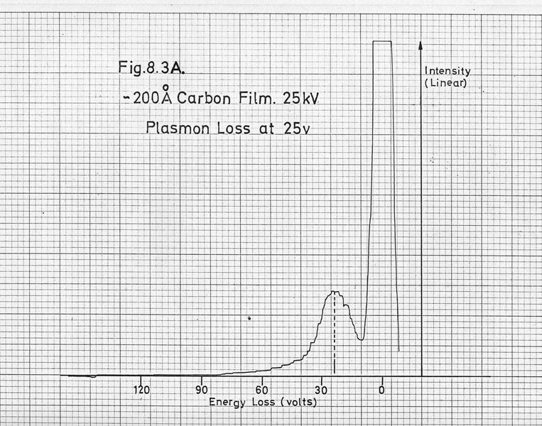
Measurements of the resolution of the filter lens showed it to be inadequate for revealing discrete losses in thin films, and Paden decided, at some sacrifice of flexibility, to depart from an axially symmetric configuration, with the construction of a dispersive type of analyser. In his new analyser arrangement, shown in [Paden, Fig. 8.1], the einzel lens operates as an electron mirror, incident and reflected electrons being separated by a transverse magnetic field. With this analyser the plasmon loss at 25 volts in a 200 angstrom carbon film was readily observed [Paden, Fig. 8.3A].
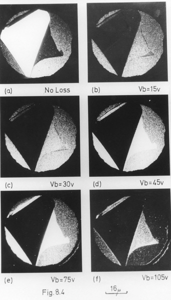
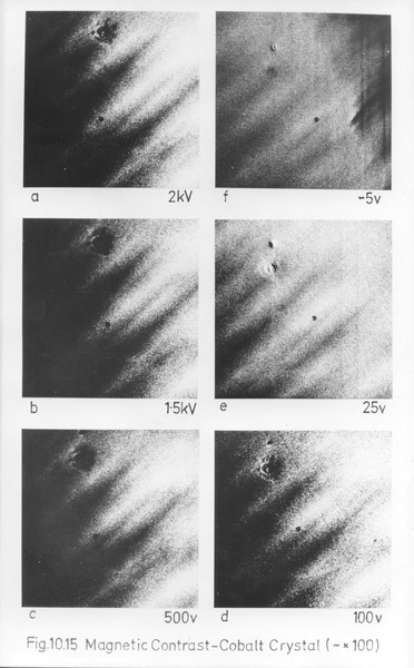
An additional advantage conferred by the mirror analyser configuration was that energy loss imaging became possible. [Paden, Fig, 8.4] is a series of scanning transmission micrographs of a carbon film, showing the changes in contrast that occur as the bias voltage of the analyser is varied. The versatile nature of the instrument allowed it to be easily converted to operate as a retarding field scanning transmission microscope. In this mode magnetic domain contrast was observed, as shown in [Paden, Fig. 10.15].
After completing his research at the Engineering Department, Dick Paden took up employment with CIC, and later moved to Camscan.
Charles Oatley probably had as early as 1954 an inkling of the potential of the SEM in microelectronics when he suggested that Smith should investigate the point-contact rectifier He and Everhart early on appreciated the significance of the observation that the signal level in the SEM was a sensitive function of specimen potential, and they developed what became known as the ‘voltage contrast’ method of investigating surface potential distributions. By the mid-1960s the SEM had become established as an important tool in the microelectronics industry. Broers and Chang were the first two students on the SEM whose projects fell within the field of microelectronics; the third was Graham Plows who started his PhD project in 1964. His task was to investigate the stroboscopic operation of the SEM, a novel method conceived by Nixon for the testing and inspection of microcircuits.
The voltage contrast method introduced by Oatley and Everhart of imaging the potential distribution across the surface of a specimen is essentially a static technique; the stroboscopic method is a dynamic technique applicable to microcircuits under operating conditions. The method may be applied to an operating circuit in two ways: in the first a stroboscopic image is obtained that provides a map of the voltage distribution across the circuit at any chosen phase of its repetitive operation, the choice of phase being continuously variable through the cycle; in the second the electron probe is stopped at a point of interest on the circuit and the waveform of the voltage at that point is displayed on the SEM screen. The latter mode of operation is akin to that of the sampling oscilloscope.
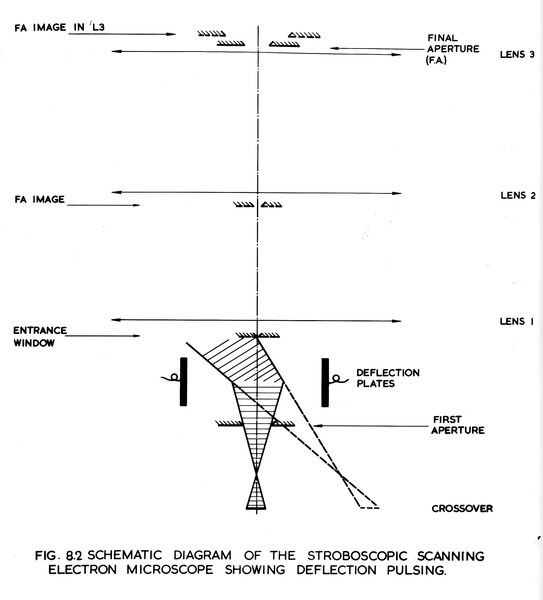
Stroboscopic operation of the SEM may be effected by a placing the sampling gate at any point between gun and display, but Plows shows, from transit time considerations, that greatest bandwidth is obtained by pulsing the electron beam in the column of the microscope. [Plows, Fig. 8.2] (Plows, 1969) shows schematically the arrangement used in the experimental instrument constructed by Plows. The beam is swept across the effective optical aperture of the system by means of electrostatic deflection plates located immediately after the anode of the electron gun. A 3.5 MHz sinusoidal voltage applied to the plates produces pulses of repetition frequency 7.0 MHz and duration 10 ns.
A schematic diagram of the stroboscopic microscope constructed by Plows is shown in [Plows, Fig. 7.11]. (This was a largely rebuilt version of the microscope used earlier by Broers and Chang.) The special electronic equipment required for stroboscopic operation comprises 3.5 and 7.0 MHz supplies for the column deflection plates and for driving the circuit devices under examination; and supplies for the electrodes of the special electron collector devised by Plows.
The arrangement of the beam pulsing and ancillary equipment is shown in [Plows, Fig. 7.13]. A variable-frequency oscillator generates power in the 3.5-3.8 MHz band, which feeds a frequency doubler and a phase changer. The output of the doubler drives the circuit devices under test, while the output of the phase changer is coupled to the deflection plates via a tuned power amplifier. The phase changer was required to allow the 3.5 MHz deflection voltage to be smoothly variable in phase relative to the 7.0 MHz output with negligible variation in amplitude. This was done by taking the output from an air-cored coil, which was rotatable in crossed fields produced by two orthogonal pairs of coils carrying the input in phase quadrature. The variable-frequency oscillator, doubler and power amplifier stages followed amateur band high-frequency transmitter practice.
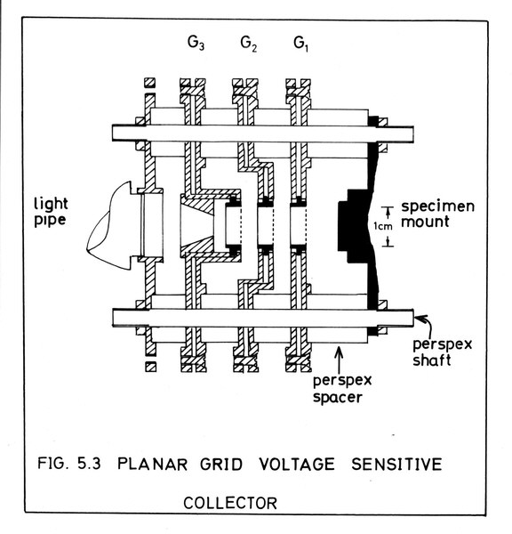
In order to place his work on a more quantitative basis Plows found it necessary to develop a new type of electron collector. The standard Everhart collector, although very sensitive to changes in surface potential, was highly non-linear and therefore unsuitable for voltage measurement. Furthermore, Plows had earlier established, experimentally and from theoretical considerations that, with the Everhart collector, effectively all of the voltage contrast at a junction resulted from return of secondary electrons to the sample by the self-field above the junction. He had concluded that the use of an accelerating electric field normal to the sample surface would reduce, or eliminate, this self-field effect. The new collector, shown in [Plows, Fig. 5.3], was designed with these considerations in mind. It contained an arrangement of three planar grids set at different voltages, and which established the requisite accelerating field. Although less sensitive than the Everhart collector, it was found to possess a substantial linear, monotonic characteristic, and reduced significantly the surface electric field effect.
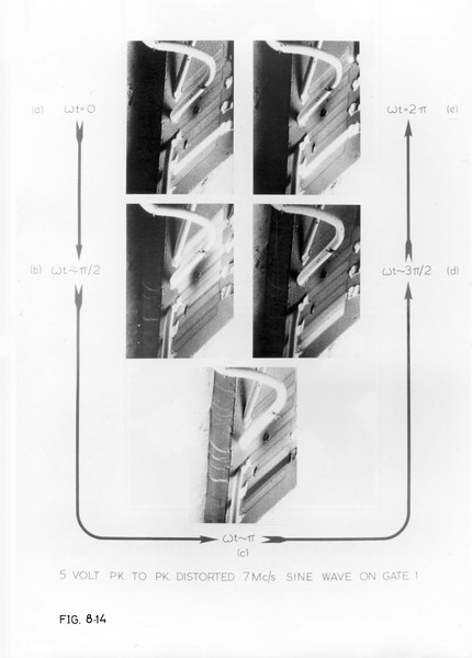
Tests on the new instrument demonstrated that it was performing according to theory. [Plows, Fig. 8.14] is the first recorded series of stroboscopic scanning micrographs showing stages in the cycle of a 7 MHz voltage waveform applied to one gate of a MOST ladder. The brightness of this gate at four instants of a complete cycle shows the expected variation.
In a series of experiments on a 24-bit dynamic shift register the probe was stationed on one of the input electrodes, and the sequence of waveforms shown in [Plows, Fig. 9.14] was recorded on a the CRT display of the microscope. The output waveforms corresponding to input pulses varying in duration over the range 10-100 microseconds showed excellent agreement with the input waveforms recorded directly on an oscilloscope.
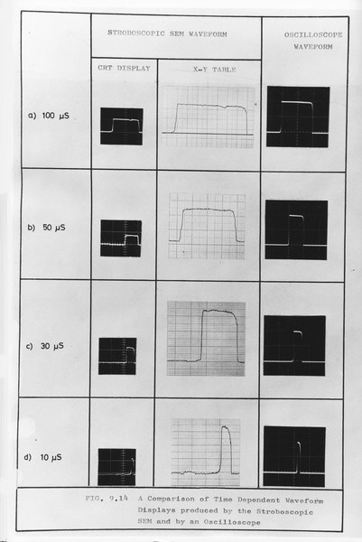
On completing his studies Plows returned to his former employer, International Computers and Tabulators (ICT), which had provided support during his PhD work. Later he took up employment with CIC, but eventually set up his own company, Lintech Instruments Ltd., to manufacture electron beam testing equipment. The first product from this company was launched in the late 1970s. Later still Lintech was purchased by CIC.
Although Barnett had earlier succeeded in revealing magnetic domains in his mirror microscope, their observation in the SEM had been a long-standing challenge in the laboratory. It was John Banbury, who commenced his PhD project in 1966, who took up the challenge. He concluded that the key to revealing microfields, including magnetic domains, at the surface of a specimen lay in the control of the electron trajectories between specimen and collector.
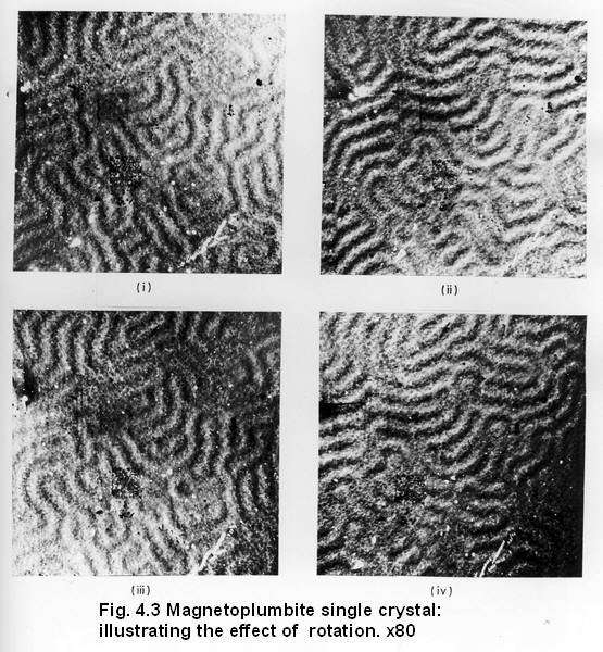
With this aim in mind, he developed, in successive stages, a new type of detector. In the first stage of this process the specimen was screened from the standard collector by an arrangement of biased plates and probes, which had the effect of shaping the trajectories between specimen and collector. By this means he was able to produce clear images of magnetic domains in the SEM for the first time. Also, by imaging the narrow gap of an energised tape head he was able to demonstrate that the vertical and horizontal components of the magnetic microfield could be distinguished. [Banbury, Fig. 4.30] (Banbury, 1970) shows how the magnetic field pattern on a magnetoplumbite single crystal changes as it is rotated through multiples of 90 degrees. The directional characteristics of the detector cause inversion of the maze pattern, and regions of low magnetic contrast become regions of high contrast and visa-versa.
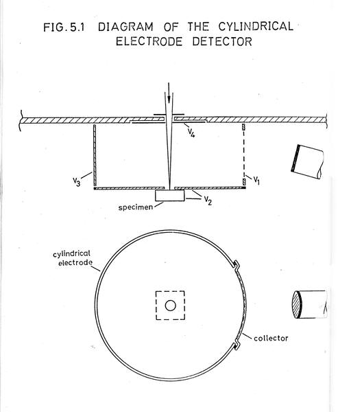
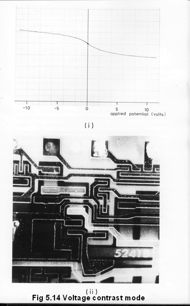
The final stage of this development was attained with the detector shown in [Banbury, Fig. 5.1]. It consists of a small thin-walled cylinder, coaxial with the electron beam, interposed between the final lens pole-piece and the specimen. Disks at each end of the cylinder have small axially located holes allowing passage of the primary beam. The specimen is mounted normally to the incident beam immediately below the second disk. Secondary electrons entering the cylinder follow curved paths to the wall of the cylinder. A proportion of these escape through a gauze-covered aperture in the wall to be collected by the nearby scintillator held at high potential. The potentials of all of the elements of the detector can be adjusted to select enhanced magnetic, voltage, or topographic contrast. [Banbury, Fig. 5.14(i)] shows the monotonic characteristic of the collected signal versus applied specimen voltage, and [Banbury, Fig 5.14(ii)] shows a microcircuit with and without an applied voltage.
The other major aspect of Banbury's work concerned the addition of a differentially-pumped UHV chamber to a normal SEM. The aim of this was to eliminate hydrocarbon contamination build-up under the electron beam and to enable studies of surface processes such as gas-solid reactions with thermal, catalytic, or electron beam stimulation to be undertaken.
The stainless steel specimen chamber was designed to be bakeable to 1800 C and the final lens was a modified to withstand a baking temperature of 120 C. A high-performance oil diffusion pump combined with a thermo electric chevron baffle was used to pump the chamber, which attained a pressure of 5x10⁻¹⁰ torr after a six hour baking cycle and six hours cooling. The aperture holder in the final lens was modified to provide a vacuum tight seal to isolate the chamber from the remainder of the column, the differential pressure being established across the 50 micron final aperture itself.
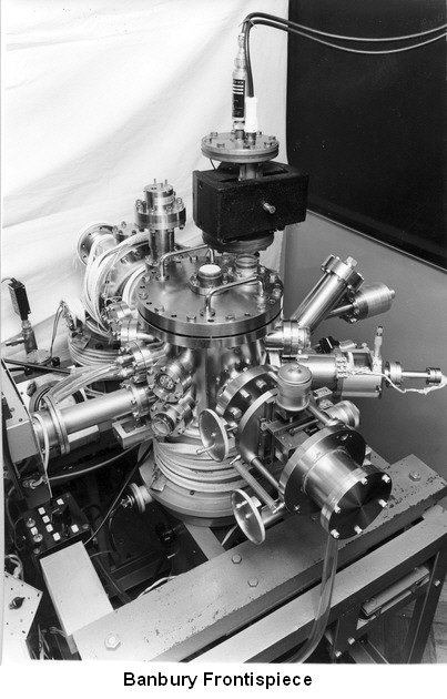
To withstand the high temperatures a polished glass light pipe together with a lithium glass scintillator were employed in the construction of the detector. Tests of resolving power before and after installation of the UHV system demonstrated that the probe size remained substantially unaffected at around 70-100 angstrom. A photograph of the UHV chamber fitted to the microscope is shown in [Banbury, Frontispiece]. A prominent feature is the elaborate specimen-stage control mechanism providing five degrees of freedom.
The UHV apparatus was used to conduct experiments involving the electron beam activated decomposition of silver chloride and stannous chloride. In one experiment a silver chloride film, 1.3 micron thick, was evaporated onto a silicon dioxide on silicon substrate, which was then introduced into the UHV specimen chamber. Pads and lines of various shapes and sizes were grown successfully. The results of a second similar experiment, using a 2500 angstrom thick silver chloride film deposited over silicon dioxide on silicon, are shown in [Banbury, Fig. 11.4]. In this experiment the probe current was approximately 10-8 ampere and exposures were of the order of 0.1 coulomb/cm2. In this series of micrographs the line widths vary between 0.3 and 0.7 micron. The experiments with stannous chloride involved the direct, in situ, evaporation of the material onto the silicon dioxide substrate while being exposed to the electron beam.
J. P. Ballantyne, who started his project in 1969, continued the work on deposition of metallic films. His objective was to investigate the process in greater detail and to demonstrate the advantages of using a system in which processing, analysis and inspection could be performed on a micro-miniature scale.
To carry out the work a number of new units were added to Banbury's original instrument, which Ballantyne inherited. These included a commercial none-dispersive x-ray microanalysis system supplied by Ortec, a pattern generator, and a gun pulsing unit. [Ballantyne, Fig. 3.1] (Ballantyne, 1972) is a schematic diagram of the complete system incorporating these extra components. The pattern generator (to a basic design by C. Dix) provided for the automatic selection and control of the areas to be exposed to the electron probe. Data for the pattern generator was read in from a short length of paper tape. The purpose of the gun pulsing unit was to blank the beam in those areas of the pattern not requiring exposure of the film. Beam blanking by applying pulses to the Wehnelt of the electron gun was preferred to an aperture sweep method, such as that used by Plows, because it entailed a substantially lower rate of electron beam induced contamination of the column.
A significant proportion of Ballantyne’s work comprised an extended theoretical discussion of the factors involved in the process of direct metallic deposition; these included the consideration of molecular dissociation, thin film and vapour flux deposition and the importance of the 'rate function'. Also considered were electron optical and electron scattering limitations, vacuum requirements, and the factors influencing material selection and preparation.
Having established a theoretical foundation for his work Ballantyne considered five potentially useful compounds for investigation, of which one, silver chloride, was selected as the most promising. This compound is reasonably volatile at moderate temperatures so that it is easy to prepare, and the deposited film adheres reasonably well to a substrate.
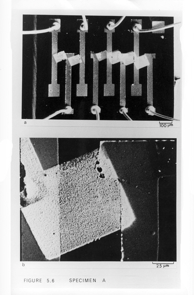
In the main series of experiments conducted by Ballantyne a film of silver chloride was evaporated on to a specially-prepared silicon oxide substrate, having on its surface an evaporated pattern of gold pads to which electrical connections could be made. Areas of the specimen, each 100 microns square, were exposed to the electron beam so as to form a bridge between adjacent gold pads. The arrangement of pads and the areas exposed to the beam may be seen in [Ballantyne, Fig. 5.6]. During deposition the silver and chlorine content of the film was monitored continuously by means of the x-ray microanalysis system, and the electrical resistance between the relevant gold pads was also monitored. Exposure of the film was stopped when no further change occurred in the silver and chlorine content and when the measured resistance stabilised.
After exposure the specimen was subjected to a chemical treatment in ammonium hydroxide which removed the residual chlorine. It also provided ‘chemical amplification’ necessary to reduce the sheet resistance of the deposited silver by a very large factor. Because the normal correction procedures used for bulks specimens in quantitative x-ray microanalysis were not applicable to the type of thin film specimens used in the these experiments, alternative methods of correcting the measured x-ray intensities were investigated. A method based on the Monte Carlo model for electron scattering was adopted. It was concluded that the correction procedures developed on the basis of this model provided at least semi-quantitative information about the degree of decomposition in the silver chloride films investigated.
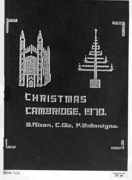
Among the applications considered for direct deposition techniques were the fabrication of resistive components, the discretionary wiring of complex integrated circuits or repair of damaged interconnections, the production of master masks, and the possibility of micro-recording. As a demonstration of the degree of complexity that might be achieved in the manufacture of masks, the picture shown in [Ballantyne, Fig. 7.11] of King's College Chapel together with a Christmas tree was drawn using silver chloride deposition. Many of these applications, however, depended on the development of an effective chemical amplification procedure requiring much further work.
In an appendix Ballantyne describes his contribution to an analysis of the cylindrical secondary-electron detector introduced by Banbury, which was undertaken jointly with Munro and Yakowitz (see Bibliography for references). Some computed equipotentials and electron trajectories are shown in [Ballantyne, Fig. A.2].
In electron beam systems for microfabrication deflection angles are large and off-axis aberrations are a significant factor in determining overall system performance. Gerry Owen commenced his PhD studies in 1971 with the object of devising improved methods for the analysis and design of deflection systems providing low values of off-axis aberrations.
The two types of probe forming system considered are defined in [Owen, Fig. 1.2] (Owen 1974): the post-lens single deflection system, and the pre-lens double deflection system. Owen began his analysis by assessing and tabulating the seven off-axis third-order aberrations associated with round lenses and the six third-order aberrations associated with deflection systems, distinguishing those which can be dynamically corrected either completely or partially. From this assessment he established a design philosophy, which was to design for minimum uncorrectable aberrations (chiefly anisotropic astigmatism and all types of coma), and then to correct the correctable aberrations dynamically.
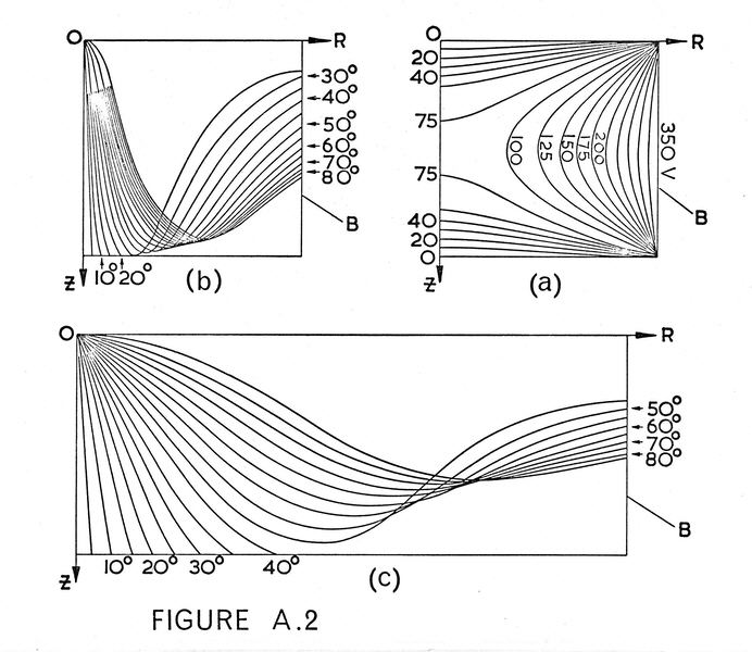
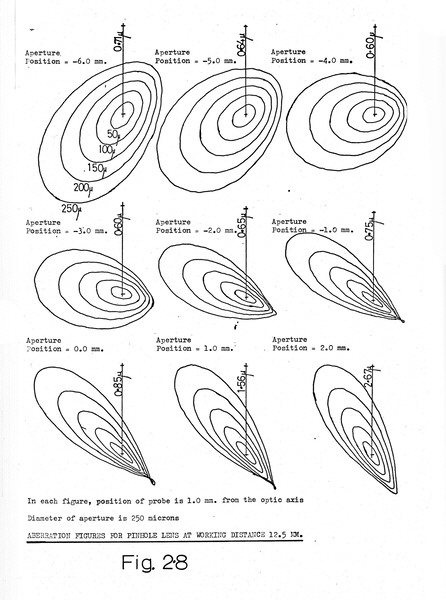
As a first step in the analysis of a complete probe-forming system, the optical properties of a typical probe-forming (pinhole) lens were determined. Munro's finite element programs were used to find the axial flux distribution from which the first and third order properties were calculated. A direct indication of lens performance is given by the aberration figures shown in [Owen, Fig. 2.8] which demonstrate that at a fixed working distance, enlargement of the spot by off-axis aberrations is a sensitive function of aperture position. Positioning the aperture near to the principle plane minimises their effects. With a pre-lens deflection system, because of the angle at which a ray enters the final lens, off-axis aberrations of this round lens need to be taken into account.
To investigate the optical properties of post-lens deflection systems the first and third order aberration coefficients were computed for a variety of coil geometries, as shown in [Owen, Fig. 3.4]. By varying systematically critical shape parameters, such as coil length, height and spacing, Owen was able to demonstrate that geometries could be found which provided very low values of both anisotropic astigmatism and coma simultaneously. A similar, but rather more complex, procedure was used to determine the optical properties and performance of a pre-lens double-deflection system.
A case study of an existing microfabrication instrument (employing pre-lens double-deflection) was then undertaken which demonstrated that because uncorrectable deflection aberrations were very large, dynamic correction would be ineffective. It was also shown that the elimination of off-axis aberration brought about by the use of post-lens single-deflection can more than compensate for the necessarily increased working distance, and hence increased spherical aberration, this entails. From these theoretical and computational studies Owen concluded that post-lens rather than the pre-lens deflection was preferable because off-axis aberrations and image rotation introduced by the final lens are thereby avoided. Additionally, post-lens systems are easier to make and easier to align since they are located in a more accessible region of the column.
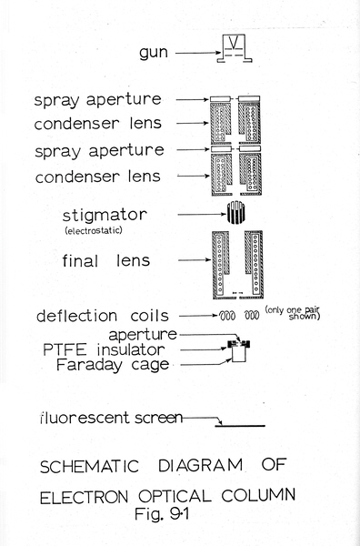
To enable comparisons to be made between theoretical predictions and measured values of spot size, an electron beam of column was assembled, as shown schematically in [Owen, Fig. 9.1]. (Components inherited from Barnett’s project were utilised for this purpose.) New components included a long-working distance lens, stages for deflection coils, Faraday cages, stigmators, grids and apertures, together with much specialised electronic equipment.
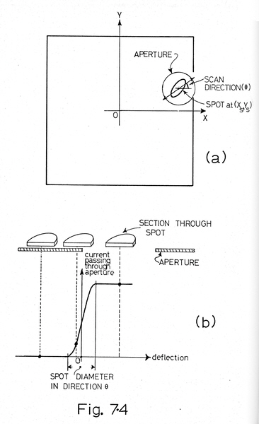
Measurements of spot size were made by scanning the focused spot across the edge of an aperture placed at defined co-ordinates in the image plane, as illustrated in [Owen, Fig. 7.4]. Spot plots, obtained by scanning the spot across the aperture at various angles, could then be compared directly with spot plots derived from computed aberration figures. Deflection coil performance was found to be critically dependent on alignment, and an elaborate procedure was devised to electrically balance each coil assembly tested and to centre it mechanically on the optical axis.
Three sets of deflection coils were constructed and used to compare experimental and computed results. One set was designed deliberately to possess moderately high aberrations, but was constructed with a precisely defined, symmetrical geometry which enabled an unambiguous computation of aberration coefficients to be made. Spot plots for these coils demonstrated very good agreement between measured and computed values. The other two sets of coils were designed for minimum uncorrectable aberrations but differed in the method of interleaving the windings. Although more difficult to construct, symmetrical windings were found to give lower aberrations.
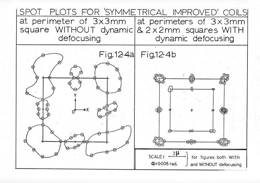
For the final phase of his project Owen derived the functions, relating coil and lens currents to aberrations, requisite for dynamic correction of isotropic and barrel distortion, isotropic astigmatism and field curvature. This was followed by the implementation of a practical scheme for the correction of field curvature. The performance of this system is demonstrated by the spot plots of [Owen, Fig. 12.4]. At the corners of a 2 mm square scan in the image plane, the measured resolution (from the spot plots) is 3 μm without dynamic correction and 0.7 μm with correction; the latter figure is in excellent agreement with the computed resolution of 0.6 μm. These figures compare favourably with a resolution of 22 μm for the 'case study' system.
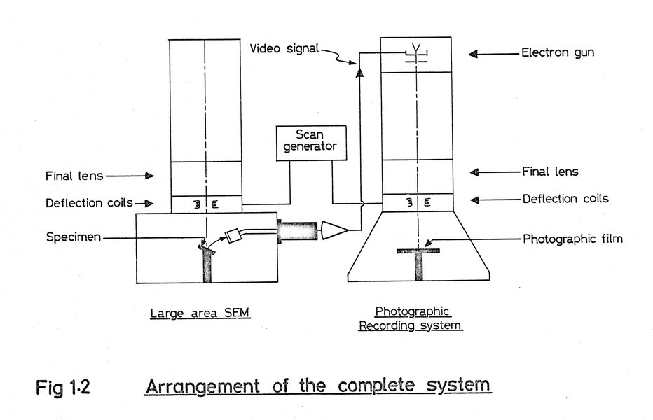
The recording of a large-field SEM images at high resolution provided the topic for Valluri (Bob) Rao's PhD work, which commenced in 1975. In the conventional SEM photographic recording from the face of a high resolution CRT provides an image definition of rather less than 10 lines per millimetre and 1000 lines per field with a very restricted grey-level range. This project aimed to achieve a resolution capability of 10,000 lines over a field of 50 mm x 50 mm. Specifically it was aimed at recording on a single micrograph the complete surface area of a VLSI chip. The system assembled by Rao is shown in [Rao, Fig. 1.2]. (Rao, 1979). It consists essentially of two complete scanning electron optical columns driven by a common scan generator. The column on the left is a large-area SEM containing the specimen chip; this part of the system was already available from an earlier PhD project. The video signal from this SEM is used to modulate the Wehnelt of the electron gun of the recording column containing the photographic film. (This electron optical column was constructed by Rao utilising components inherited from Barnett’s project.) Both columns feature post final-lens deflection coils, since at the large deflection angles involved in this application the deflection aberrations arising with a conventional pre-lens deflection system would be excessive.
A major part of Rao’s project was concerned with the establishment of the aberration theory requisite for the design of the high-resolution large-area deflection system, and of the computation of its optical properties. Aberrations arising in the deflection system, and considered in the theory, are illustrated in [Rao, Fig. 2.1]; the design procedure aimed to minimise both third and fifth order aberrations since for this application deflection angles are very large. Computer programs were written to calculate the field parameters, the first order properties and the third and fifth order aberration coefficients. Programmes were also developed for the evaluation of the probe shapes and a probe sizes for arbitrary gaussian deflections and angular apertures. A novel method of re-grouping aberration coefficients was devised which effected a considerable reduction in the number of coefficients that needed to be considered and which greatly simplified the design procedure.
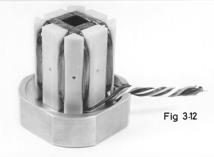
The theory revealed that the performance of the deflection coils was a very sensitive function of coil length and of the working distance to the plane of the photographic film, conclusions that were confirmed experimentally. By optimising the coil geometry and working distance the magnitude of the dynamic lens current correction required to compensate for field curvature and thus maintain probe focus was reduced to a small percentage. A photograph of the coil assembly is shown in [Rao, Fig. 3.12].
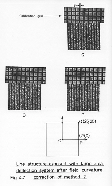
An assessment of the optical performance of the deflection coils was obtained by scanning the focused probe over a 50 mm square area of film in a series of rasters with varying line definition. Examination of the exposed line widths with an optical microscope provided a sensitive method of detecting variations in the probe size. [Rao, Fig. 4.7] shows three regions of an exposed negative demonstrating the uniformity of line structure at the extreme edges of the raster where a probe size of less than 5 μm was achieved. In addition, it was observed that a variation in the exposed linewidth, due to aberrations, caused a change in the optical density of the developed negative. This phenomenon, which was attributed to the non linearity of the optical-density versus electron exposure relationship, provided an additional novel means to assess rapidly the deflection aberrations. Measurements were also made of the electron sensitivity of the photographic emulsion used, its line spread function, DQE, grey-level capability and other parameters.
Correct operation of the electron gun proved to be a critical factor in the overall performance of the recording system. Measurements of the Wehnelt voltage/probe current modulation characteristic revealed that anode misalignment could result in a highly non-linear, non-monotonic characteristic. To correct for this an alignment procedure was developed involving the monitoring of the modulation characteristic on an oscilloscope. This same procedure was also used to set up the gamma correction circuit required to compensate for the inherent non-linearity of the modulation characteristic. For a carefully aligned gun no shifts of the probe could be observed, and defocusing effects due to modulation were found to be insignificant.
To complete the project the recording system was coupled to the large area SEM, as illustrated in [Rao, Fig. 1.2], and used to obtain a comprehensive series of micrographs of integrated circuits. Recordings were made using a line scan rate of 200 Hz and a frame scan time of 50 s resulting in a definition of 10,000 lines. [Rao, Fig. 8.2], typical of the series, shows a 5 mm square area of an MOS random access memory. The smallest feature is 4 μm. An interesting aspect of this micrograph is that beam penetration has revealed the individual layers of the chip.
Investigations relating to the application of electron beam techniques to the study of operating integrated circuits were continued in 1982 by Simon Garth whose research was arranged as a collaborative project with Texas Instruments Ltd., Bedford. To provide the basis for the investigations a new Cambridge Instruments S-200 SEM was purchased together with an electron beam detection subsystem from Lintech Instruments Ltd., of Cambridge. This combination was considered to be state-of-the-art at the time.
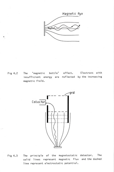
In an extensive review of previous work and the limitations of existing systems, Garth concludes that distortion of the emitted electron spectrum resulting from local electric fields close to the surface of an integrated circuit is a major limitation to the attainable voltage resolution. Moreover, as circuit features shrink, so the problem will increase. A critical analysis of the most common type of retarding field spectrometer, in which an extractor electrode is placed near to the sample, shows that this can only partially alleviate the local field effect. Garth points out that all of the previous designs considered have been entirely electrostatic and can only influence electrons as a function of field strength at their local position. His unique solution to this problem was the 'magnetostatic' detector in which electrons are focused parallel to the axis of the system before they reach a planar collector. Such an arrangement acts as a total energy spectrometer and minimises the effect of angle modulation caused by local fields.
The principal of the magnetostatic detector is shown in [Garth, Fig. 4.3] (Garth, 1985). The sample is located in the field of a single-pole lens. Secondary electrons are guided along the magnetic field lines, travelling almost parallel to the axis into the detector. By this means the total velocity of the electrons is measured and not just the component in the axial direction. In contrast to previous designs the magnetostatic detector needs no extraction potential to guide the electrons to the detector, which makes it more suitable for studying passivated devices.
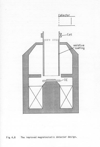
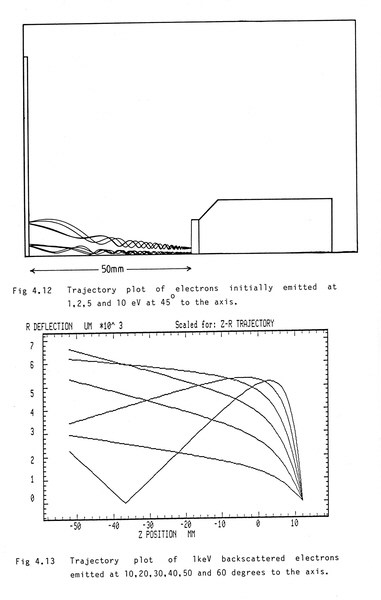
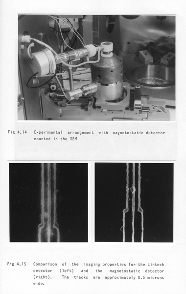
Garth's implementation of the magnetostatic detector in its final form is shown in [Garth, Fig. 4.8]. It was designed with the aid of the CIELAS programs, suitably modified for this purpose. Electron trajectory plots are shown in [Garth, Fig. 4.12]. The detector is mounted on the normal specimen stage of the SEM, below the objective lens, the primary beam being focused either by the single-pole lens, the SEM objective, or a combination of both. [Garth, Fig. 4.14] shows the experimental arrangement and [Garth, Fig. 4.15] compares the imaging properties of the new system with that of the original Lintech system.
In order to assess the local field rejection properties of the new detector a special test chip was made having a series of tracks of variable widths and spacings to which arbitrary voltage waveforms could be applied. Tests using this chip confirmed that the magnetostatic detector reduced the effects of local fields by at least an order of magnitude over the purely electrostatic Lintech detector. Following the success of the initial design further work was carried out using computer modelling and simulation to predict the performance of a proposed semi-optimised design.
To further extend the investigations Garth led an undergraduates final year project aimed at producing a prototype electron beam test system based on a GEMS framestore (see Smith ) and image processing unit. The system employed the 'logic latching' principle and provided the basis for an image based logic analysis workstation. Finally, the methodology of electron-beam voltage measurement was considered, and more rigorous techniques were proposed for implementation in future electron beam testing equipment.
While investigating the effect of the electron beam irradiation on the operating characteristics of devices, Garth observed a shift in the drain threshold voltage required to initiate conduction. This led him to propose a new type of circuit device which he termed a TRAPMOS (trapped charge MOS, Brit. Pat. No. 84 - 00332). A complimentary structure, termed a TRIMOS (tri-state MOS), consisting of two of these devices was also proposed. These new devices may have potential applications in analogue circuitry and in circuits where low power dissipation is important, although further research and development will be required.
The investigations on electron beam testing were continued in 1985 by John Thong. In an exhaustive review of current technology he identified the fundamental factors which determine the upper limit to the sampling frequency in the stroboscopic mode. A key parameter is the duration of the electron pulse and this is limited fundamentally by the energy spread in the beam. By extending earlier theoretical work Thong showed that energy spread induced by beam deflection in the chopping element is a significant contributing factor to the total energy spread, which becomes significant at the picosecond pulse durations and low beam accelerating voltages (1-2.5 kV) requisite for high-speed testing. This theoretical work was supported by experiments conducted using the Cambridge S-200 SEM inherited from Garth to which a new high-speed parallel plate deflection unit was added together with equipment to measure pulse duration, beam energy spread and other parameters.
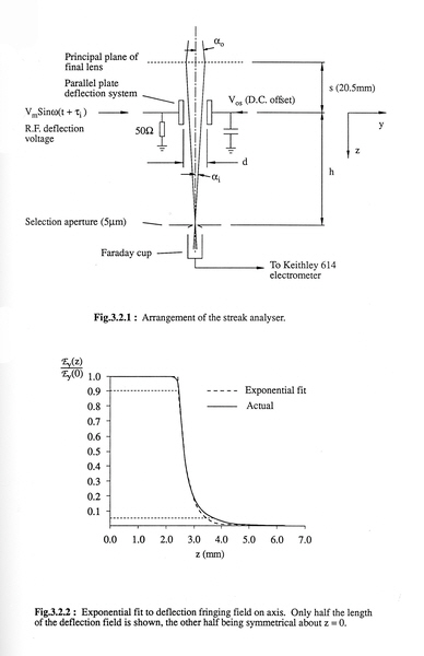
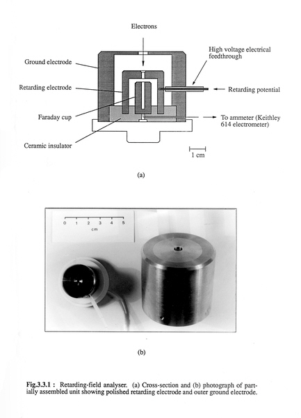
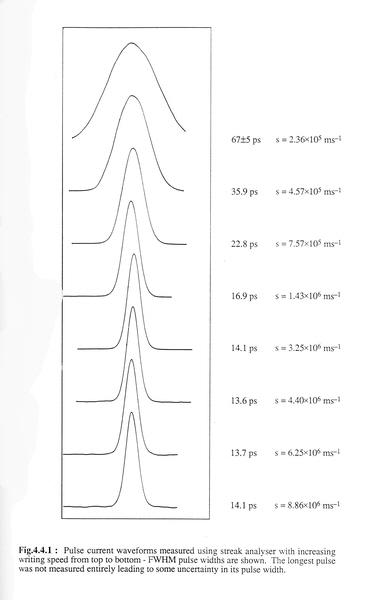
In order to measure pulse duration the method shown in [Thong, Fig. 3.2.1.] (Thong, 1989), based on the streak camera principle, was adopted. This Thong considered was the only viable option providing sufficient temporal resolution to resolve picosecond pulses. Measurements of energy spread were made by means of the three-electrode retarding field analyser shown in [Thong, Fig. 3.3.1]. Pulse current waveforms measured using the streak analyzer are shown in [Thong, Fig. 4.4.1]. Measurements of energy spread distributions with and without beam chopping, shown in [Thong, Fig. 4.4.2], demonstrate the broadening due to deflection.
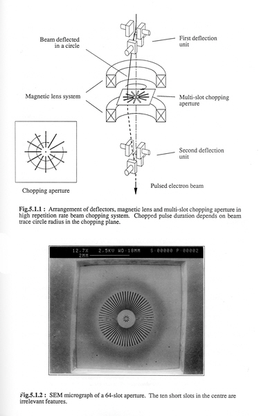
Pulse production with conventional deflection chopping techniques is limited to repetition rates of a few GHz at low beam energies because the finite electron transit angle through the deflection field causes loss of deflection performance at higher frequencies. Difficulties are also encountered when attempting to drive deflection systems at ever higher microwave frequencies. To circumvent these problems Thong developed a novel beam deflection chopping system the principle of which is shown in [Thong, Fig. 5.1.1]. An arrangement of parallel plate deflectors and a magnetic lens is used to cause the beam to execute a circle in the plane of a multi-slot chopping aperture. The elements are arranged so that there is no net deflection of the beam. The multi-slot aperture is fabricated in a silicon membrane to very high precision using electron beam lithography techniques.
With a 64-slot aperture and a driving frequency of one GHz on the deflectors, time-resolve measurements of electron pulses demonstrated a pulse period of 15.6 picoseconds corresponding to a repetition frequency of 64 GHz. Experiments were conducted using a beam trace circle radius of 0.4 - 1.0 mm. Waveform measurements of an 18 GHz sinusoidal signal on a test coplanar wave guide clearly demonstrated the viability of the system.
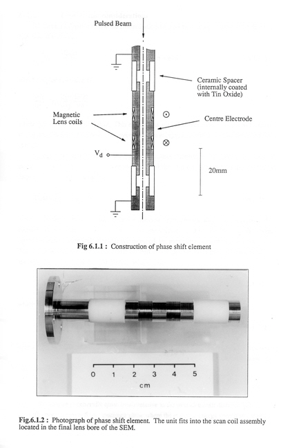
In existing electron beam sampling methods phase shift is generally achieve by delaying the electrical signals that drive the beam pulsing system, a technique suffering from serious shortcomings, in particular jitter, at high frequencies. Thong addressed this problem by introducing a new electron optical phase shift element, which produces a controlled, variable delay in the electron pulse stream. The element, shown in [Thong, Fig. 6.1.1] comprises a uni-potential electrostatic lens together with a superimposed electromagnetic lens field generated by two contra-wound coils. By varying the voltage on the centre electrode of the electrostatic lens the electron flight time may be changed and thus the pulse delay. The operation of the element was verified experimentally via both time resolved pulse measurements and waveform measurements using the basic stroboscopic SEM system.
An important effect contributing to waveform measurement error in the testing of high-speed devices, the 'Transit Time Effect', was also investigated by Thong. This effect arises because time-varying signals on a device under test give rise to dynamic electric fields that affect the energy of secondary electrons in transit between the device and the extraction grid of the spectrometer. Energy changes become significant when signal variations occur on a time-scale comparable to the electron transit time. The effect was analysed by Thong by evaluating the secondary electron spectrum for a range of device structures and operating parameters. This was carried out in a Monte Carlo simulation for a large number of trajectories with the starting parameters of the electron beam weighted by the distribution functions characteristic of the emission process. Results from these simulations were in agreement with experimental results obtained for a coplanar wave guide structure.
REFERENCES
Ballantyne, J. P. (1972). Scanning electron beam controlled direct metallic deposition. Ph.D. Dissertation, University of Cambridge.
Banbury, J. R. (1970). Control of the specimen environment in a scanning electron microscope. Ph.D. Dissertation, University of Cambridge.
Barnett, M. E. (1966). Mirror electron microscopy. Ph.D. Dissertation, University of Cambridge.
Buchanan, R. (1964). An electron optical bench for electron microscopy and x-ray microanalysis. Ph.D. Dissertation, University of Cambridge.
Garth, S. C. J. (1985). Electron beam testing of operating integrated circuits. Ph.D. Dissertation, University of Cambridge.
Owen, G. (1974). The analysis and design of probe forming systems for microfabrication. Ph.D. Dissertation, University of Cambridge.
Paden, R. S. (1967). Scanning and transmission electron microscopy with energy analysis and variable impact energy. Ph.D. Dissertation, University of Cambridge.
Plows, G. S. (1969). Stroboscopic scanning electron microscopy and the observation of microcircuit surface voltages. Ph.D. Dissertation, University of Cambridge.
Rao, V. R. M. (1979). Direct recording with electron scanning. Ph.D. Dissertation, University of Cambridge.
Thong, J. T. L. (1989). Electron beam testing technology for high-speed device characterisation. Ph.D. Dissertation, University of Cambridge.