V. RESEARCH DIRECTED BY C. W. B. GRIGSON ![]()
Contributed by D. McMullan.
A. Electron Diffraction Camera
B. Scanning Electron Diffraction
Christopher Grigson joined Charles Oatley's laboratory in the Cambridge University Engineering Department in 1950 as a post-graduate research student, having done well in both parts of the Mechanical Sciences Tripos. He was the third of Oatley's students, following K. F. Sander and D. McMullan, to undertake the building of an electron optical instrument and it is probable that Oatley would have liked to have him work on the SEM. However, it was too soon to know whether McMullan's research would bear fruit and merit further work, and instead Oatley gave him the task of building an electron diffraction camera (McMullan, 2004).
Quoting from the introduction to Grigson's dissertation (Grigson, 1955):
"The subject selected for research was the design of an electron diffraction camera and its use for the investigation of thin films important in electrical engineering.....
"A survey of the literature soon showed that it was possible to build instruments of far higher resolving power than that of the simple single lens cameras made before the war; it also became clear that a high resolving power would be desirable for the study of the size of the film particles. The first two and a half years were taken up with the design and development of the instrument. The experiments on thin films were done during the summer of 1953. The interpretation of the diffraction patterns and of the behaviour of the films took a year more, though the work was no longer carried on full-time [because of teaching duties, eds.].
"A diffraction instrument with an electrostatic optical system has not previously been described. The instrument and the associated apparatus .......... were designed subject to the specifications laid down for the camera by Mr C.W. Oatley. One of these, that evaporation must be done outside the main body of the camera, turned out to be very important for the solid state research for it meant that there should be no ambiguity as to whether changes in the film took place as a consequence of migration in some unknown way of the film material. ...... Some of the results of this study are thought to be new: namely for a twin lens instrument the resolution attainable is nearly independent of the specimen to plate distance; that the voltage stability requirement for instruments designed for particle size determination is stringent; and the special requirements for guns. The correct position of the lenses for a twin lens instrument was worked out independently and used for design. It has since been confirmed by Cowley and Rees (1953). ....."
In the last chapter of his dissertation some of his results are summarised including:
"......... this survey has revealed the important features of the way the alkali halides LiF, NaCl, and KCl grow in thin films. Namely that growth does not take place as it does in metals by the gradual appearance of myriads of crystals which increase in size at one another's expense, but by the appearance of "full grown" crystals here and there in the melt, and the gradual change of the melt to the crystalline phase as a result."
It is clear from his dissertation, which he submitted at the beginning of 1955, that he had not taken part in the SEM research. In 1953 he had been appointed University Demonstrator so that teaching was taking up a fair proportion of his time, and even more so when he was promoted to Lecturer in 1956 and elected to a Fellowship at Trinity College.
B. Scanning ElectronDiffraction
A year afterwards, he took over from Oatley the supervision of Oliver Wells who was in the fourth year of his SEM research project. This may well have fired his interest in scanning techniques because some time later he started work on a fast scanning electron diffraction system (SEDS) following the publication of the description of such an instrument by Bagdyk'yants and Alekseev (1958) in the USSR. His first SEDS began operating in May 1961, and he reported this in a letter to Nature the following November (Grigson, 1961):
"An electron diffraction system for the quantitative investigation of rapid phase changes in solids has recently been completed. The system will record an electron diffraction pattern of the Debye-Scherrer ring type in 50 msec., giving the electron intensity at the peaks of strong reflexions to an accuracy of 2 per cent. The system gives an improvement in speed of direct recording of about 4 orders of magnitude (Bagdyk'yants and Alekseev, 1958), and is thus attractive for investigating quantitatively rapid changes in solids such as polymorphic transformations, transitions from the amorphous to the crystalline state, diffusion in alloys. It is also suitable for investigating controversial questions in electron diffraction such as the transition from geometrical to dynamic diffraction conditions."
There follow two examples of its application to a polycrystalline gold film and to a high-speed amorphous-to-crystalline change in a film of silver in response to sudden heating.
"The ultimate speed of recording in such a system is set by the shot noise in the diffracted beams. The limitations are the same as those of the scanning electron microscope. Measurements show that the intensities at diffracted peaks are about 10-9 amp. Thus, for an accuracy of 1 per cent at such a peak, a picture point may be recorded in about 2 µsec. One may expect the recording times for a complete diffraction pattern of 1 msec are a question merely of improvements in technology."
This letter was followed about 6 months later by a paper with a full description of the instrument:
“This is an account of a new instrument for solid-state investigations: the fast scanning electron diffraction system (Grigson, 1962). It includes a description of the first model which began operating in May 1961: treats the factors which limit the performance of such systems; and gives a discussion of typical results, and of applications where such instruments are an advantage”.
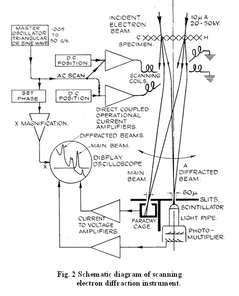
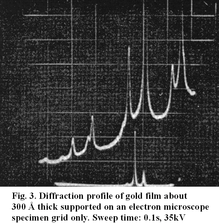
[Grigson, Fig. 2] is a schematic diagram of the instrument developed by Grigson (1962), and [Grigson, Fig. 3] is a typical diffraction profile of a 30-nm gold film.
In October of 1961 Grigson’s first research student, P. N. Denbigh, who had taken Parts I & II of the Mechanical Sciences Tripos, started his project, which was to use the instrument and to make improvements including the addition of a velocity filter.
P. N. DENBIGH
In the Introduction to his dissertation, Denbigh (1964) wrote:
“......The advantages of a Scanning Electron Diffraction System (SEDS) over photographic instruments are essentially two-fold:
1) the recording speed is high, well suited for observing solid-state changes. As originally designed, the equipment can display the essential information of the diffraction pattern in 50 msec.
2) the intensity is recorded directly. In conventional diffraction cameras the picture is recorded on on a photographic plate and the intensities must be determined photometrically from the density of blackening. In the SEDS a direct recording of the intensity is given by the height of the trace on an oscilloscope.
“One particular problem of electron scattering, at present under much discussion is the effect of inelastic scattering on the resolution and contrast of electron micrographs. The total inelastic scattering distributions and the scattering cross sections are not known experimentally. The mechanism of energy loss is not yet properly understood. If the inelastic electrons are to be studied they must first be separated from the elastic electrons with some form of filter.
“ The SEDS gives direct measurement of scattered intensity. With the addition of a velocity filter for the exclusion of electrons which have experienced more than a selected energy loss, an exceptionally powerful tool is available for the investigation of inelastic scattering. If all the inelastic electrons are removed, a very clear insight into elastic scattering is also possible.
“The development of the SEDS described in this dissertation is mainly devoted to the addition of a high quality velocity filter (VF) capable of transmitting electrons of less than a chosen electron loss. The adaptation of this filter into a velocity analyser capable of displaying electrons of a particular energy loss, is also described.”
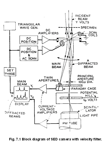
A block diagram of the SEDS with a velocity filter is shown in [Denbigh, Fig. 7.1].
Denbigh used the SEDS in 4 ways:
(1) Clarification of diffraction profiles by excluding inelastically scattered electrons with the VF.
(2) The study of background scattering in elastic profiles.
(3) Study of inelastic scattering.
(4) Study of discrete energy losses in aluminium and the variation as a function of angle.
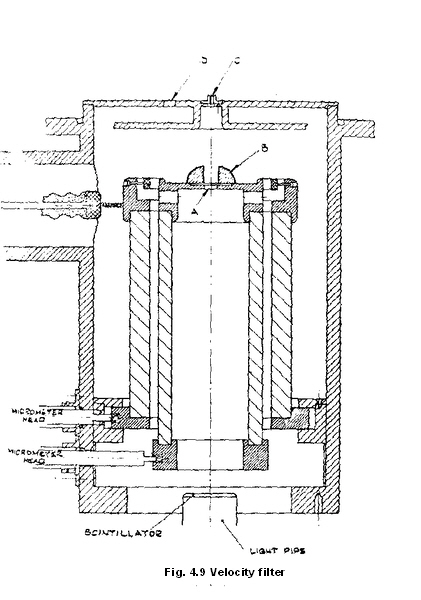
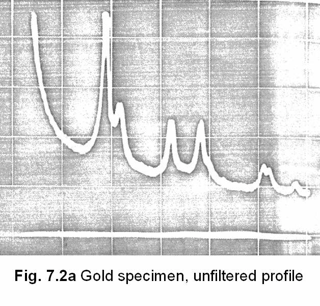
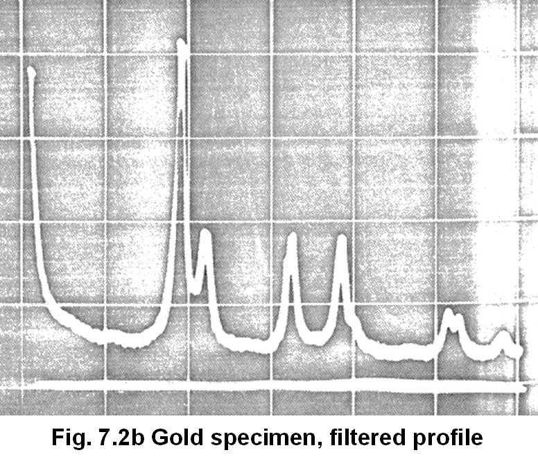
He carried out a comprehensive survey of the various types of velocity filter and decided on a non-imaging filter consisting of a fine wire mesh, initially 50 lines per inch for first tests, and then increased to 1500 lines per inch (silver wire). A cross-section of the filter ([Denbigh, Fig. 4.9] shows the micrometers for mechanical alignment which was very critical. [Denbigh, Fig. 7.2a] is the diffraction profile (electron energy 30 keV) from a 30-nm gold specimen without filtering, and [Denbigh, Fig. 7.2b] the filtered profile with the inelastically scattered electrons suppressed.
Specimens of various thicknesses were supplied by Dr R. P. Ferrier of the Cavendish Laboratory and Denbigh successfully compared the experimental results with a theory he had originated for evaluating the total inelastic scattering cross-sections. And he adapted a technique, called A.C. sorting, which had been devised by Leder and Simpson (1958) for studying the energy spectrum of the central spot in electron scattering experiments, and used it to display complete diffraction profiles for a particular energy loss.
Denbigh summed up his work as follows:
“The most significant chapters of the dissertation are on:
1) Elastic profiles where improved detail is shown to be visible when the velocity filter is used.
2) Inelastic background scattering where an important interpretation of large angle scattering is given. The interpretation leads to a method for evaluating the mean free path for all inelastic processes.
3) A.C. sorting which displays diffuse rings, corresponding to electrons with certain discrete energy losses, near the central spot. The diameters of these rings and the energies to which they correspond are important evidence of the type of inelastic scattering process.”
Grigson started a year’s sabbatical leave at the end of 1964, after Denbigh had completed his research, and spent it in the USA at Bell Telephone Laboratories, Murray Hill NY, where he continued his work on SED with D.B. Dove and G.R. Stilwell. With them he built an SEDS similar to the Cambridge instrument except that a magnetic filter was used initially (Grigson 1965) and a mesh filter was substituted later. This was done with the help of Denbigh who submitted his dissertation in 1964 and later was at Bell Labs for a period. He was a joint author of a number of later publications: Denbigh and Grigson (1965); Denbigh and Marcus (1966); Dove and Denbigh (1966); Denbigh and Dove (1967).
M. B. HERITAGE
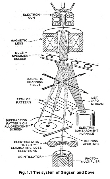
Marcus Heritage took over Denbigh’s SEDS1 in October 1964 and made a number of improvements: to the vacuum system, to the furnace used for evaporating thin specimen films, and to the mesh energy filter (he acknowledged that “this is a direct consequence of the
earlier work of Grigson and Dove [Heritage, Fig. 1.1])”. In his dissertation he wrote:
“The main aim has been to develop the SEDS as a tool for thin film studies. The instrument,
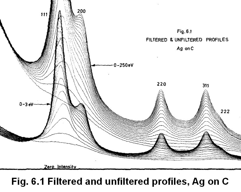
even in its modified form, was not suitable for the quantitative correlation of the theories of heterogeneous nucleation. However, the methods of analysis that are developed in this dissertation, have particular relevance to this problem.... The aim has been to apply the high measurement accuracy of SED to the earliest stages of thin film growth... The problems and advantages in calculating the radial distribution function (RDF) of very thin films were considered... The work has been made possible by the ability of the SEDS to record accurate, energy diffraction profiles, e.g. silver on carbon [Heritage, Fig. 6.1], combined with the ever expanding capability of electronic computers to transform the data into usable real-space terms. Certainly SED provides a method of recording diffraction data which is ideally suited to digital processing.
“In [Heritage, Fig. 6.1] the differences between the elastic and total scattering profiles were examined by the following procedure. Silver was deposited on carbon for a given period. The filtered profile was then recorded for half the scan cycle, and likewise a partially-filtered profile on the return scan. Film deposition was then allowed to continue, and the whole procedure was repeated. The Figure shows the resulting sequence of measurements with energy loss bandwidths 0-3 eV and 0-250 eV respectively. The latter covers the loss bandwidth of most inelastically scattered electrons, and gives measurements which are virtually unfiltered. Each trace corresponds to an increment of 2.5Å mean thickness. The zero intensity line is common to both families of curves.
“In addition to the obvious rise of measured intensity as the filter bias increases, [Heritage, Fig. 6.1] illustrates several important differences:
(a) The background intensity between the diffraction peaks of the unfiltered curves is about 4x that of the filtered ones.
(b) The final “elastic” diffraction profile shows an intensity maximum. Any further increase in mean thickness results in reduced intensities. The unfiltered traces show no sign of reaching such a maximum.
(c) The filtered profiles show the intensity for s < 0.34 Å-1 to decrease with mean thickness. The intensities of the 0-250 eV traces increase in this angular range for all but the final stages of growth.
(d) The half-widths of the filtered peaks are less than those of the unfiltered peaks.
“One can envisage the future of the scanning electron diffraction system, not so much in terms of completely new developments, but more as a combination of existing techniques into one instrument. Ferrier and Curtis, and also Bradbury, have already shown the feasibility of introducing SED into a conventional transmission electron microscope. The addition of an ultra-high vacuum specimen chamber to such an instrument is the next obvious step towards the quantitative interpretation of the nucleation and growth of thin films. The contribution of small angle scanning electron diffraction should be most useful in this field, although it must be used in conjunction with accurate measurements of the true specimen temperature and of the film deposition rate”.
Heritage was a joint author of two published papers: Grigson et al. (1966) and Tompsett et al. (1967).
M. F. TOMPSETT
In 1962, one year after Denbigh started work on SEDS1, Michael Tompsett joined Grigson’s group and commenced the building of a reflection SEDS for surface analysis. This was
largely a second copy of Grigson’s original instrument with some of Denbigh’s
modifications, in particular the mesh energy analyser. Although he wished it to operate at UHV, this would have been too expensive and he limited his changes to reducing the number of ‘O’ ring seals.
He considered various types of energy filter and reached the same conclusion as Denbigh that the mesh filter was the most suitable, and the simplest. He improved the design so that the alignment was not so critical and reduced the noise due to surface charging of the insulator.
The original Grigson SEDS used a single magnetic lens to produce an angular half-width of the final spot of 10-3 radians for observing polycrystalline specimens. Tompsett intended to examine single-crystal patterns and the observation of small angle scattering from transmission specimens, for which he needed a final spot half-width of 10-4 radians. He therefore decided to use a two-lens system.
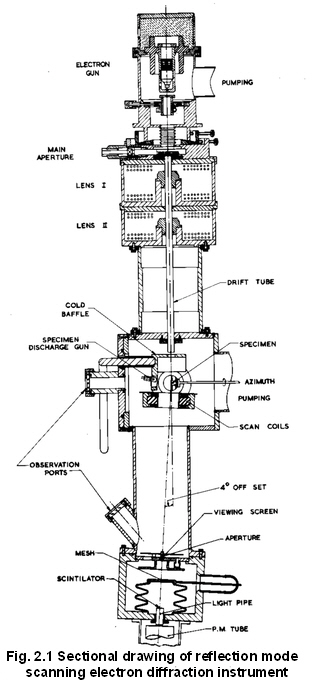
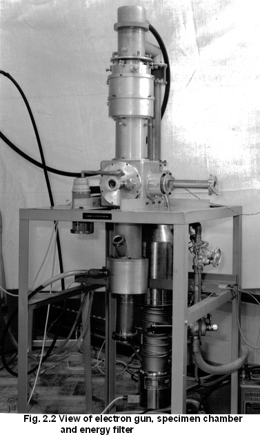
A sectional drawing of the instrument is shown in [Tompsett, Fig. 2.1] and a photograph in [Tompsett, Fig 2.2]. The specimen chamber accommodated a specimen holder, scanning coils and cold baffle (cooled with LN2). The specimen (1) could be changed through an airlock by pulling back the holder shaft (2) through a tube with a section at backing pressure sealed by ‘O’ rings. The holder provided two translational and two rotational degrees of freedom.
Tompsett made a very critical assessment of the performance of the completed SEDS and introduced improvements when time permitted. He incorporated a 3-dimensional display technique:
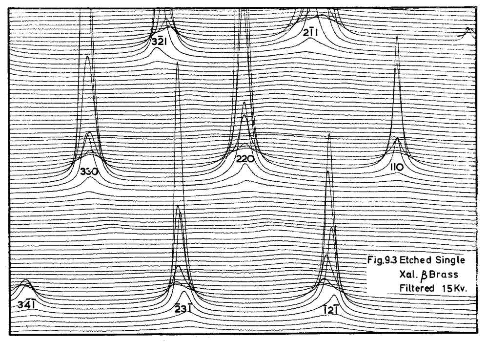
“Single crystal or preferred orientation electron diffraction patterns cannot be characterised by a single radial scan, therefore a 3-dimensional display system was developed. The angular position coordinates are derived from the currents through the orthogonal pairs of scan coils by feeding proportional signals into the X and Y channels of the [pen] recorder. By adding the intensity simultaneously into the Y channel three-dimensional displays become possible.”
[Tompsett, Fig. 9.3] shows the filtered display from a single crystal of etched β-brass. These results were published in a Nature letter (Tompsett and Grigson, 1965). He also measured scattering from amorphous materials and worked out a theory of diffraction contrast from smooth surfaces.
Tompsett completed his research in August 1965 (Grigson was on sabbatical leave at Bell Labs for much of this last year and Tompsett was being supervised by Oatley). After leaving Cambridge, he was a co-author of three further published papers: Tompsett and Grigson (1966), Grigson et al.( 1966) and Tompsett et al. (1967).
P. I. TILLETT
In 1965 Grigson returned from Bell Labs where he had worked with D.B. Dove on the design of an improved SEDS (Grigson and Dove 1966). P. I. Tillett, who started research at CUED in October 1965, was given a project “which was aimed at studying the earliest stages of thin film growth at cryogenic temperatures under conditions of very high vacuum.”
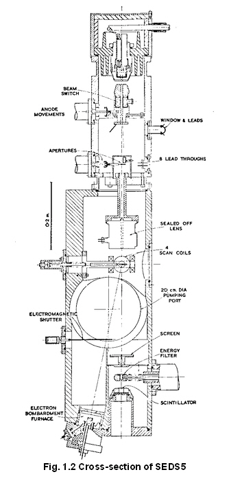
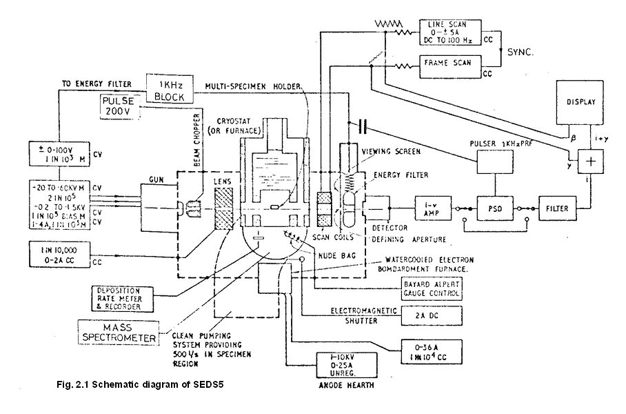
A schematic diagram of SEDS5 is shown in [Tillett, Fig. 1.1] and a cross-section in [Tillett, Fig. 2.1]. The basic design of this instrument had been completed by Grigson in the summer of 1965. “Compared with the previous instruments, filtered diffraction profiles were to be obtained under better conditions of vacuum (10-8 Torr) and operating at higher voltages (70 kV). The system was to be capable of accepting a liquid helium cryostat in which thin films could be grown under carefully monitored conditions.” A compromise had to be reached between cost and performance: a fast mercury diffusion pump (1500 l/s) with a double LN2 trap was used and all seals were made with ungreased Viton "O” rings or stainless steel bellows where movement was required. Baking could be carried out to 150 ºC. A mass spectrometer was included; the best pressure attained was 7 x 10⁻⁸ Torr after a bake.
The electron optics was similar to the earlier systems except the magnetic lens was in a sealed enclosure. The velocity filter was simplified and it was found that the mesh could be replaced by a single small aperture.
Thin specimen films were evaporated in situ using a 2 kW electron bombardment furnace which was watercooled to reduce outgassing. Film thickness was monitored with a quartz crystal oscillator microbalance. Films of Pb, Fe, Sn, and Bi were studied.
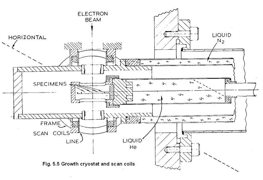
A liquid helium cooled stage holding up to six specimens was incorporated [Tillett, Fig. 5.5]. Tests were made by condensing hydrogen on a thin carbon substrate and the diffraction profile showed the growth and decay of a thin film of hydrogen and indicated that the temperature was less than 6 ºK. It appears that these were the first transmission electron diffraction measurements to be obtained from solid hydrogen
Radial distribution analysis (calculation of the population of atoms as a function of the radius from an average atom) was applied to nucleation studies of Pb films at 5ºC and 20ºC and Fe at 25ºC.
Grigson left Cambridge for an appointment in Norway at the end of 1966 and the supervision of Tillett was taken over by Prof A. H. Beck for the remaining 2 years. However Grigson continued to be in contact and he, with Tillett, published two paper on Tillett’s research (Grigson and Tillett, 1967; Tillett and Grigson, 1967) and a third surveying the SEDS work at CUED since 1962 (Grigson and Tillett, 1968).
F. C. S. M. TOTHILL
At the end of 1964, while Grigson was at Bell Laboratories, the Engineering Department was approached by the Royal Radar Establishment (RRE) with a proposal to modify a transmission electron microscope to permit the in-situ growth of'evaporated thin films in an improved vacuum. This fitted in well with Grigson’s intention to improve the SEDS instruments, and a new research student commenced work in 1965; he was F. C. S. M. Tothill and in his first year he was supervised by Grigson and then by Nixon, although Grigson who was in Norway continued to take an in interest. The following account is taken from Tothill’s Dissertation:
“A draft proposal was drawn up by C. W. Oatley, C. W. B. Grigson and W. C. Nixon for an instrument with the following specifications: (i) a pressure of 10-8 Torr, preferably 10-10 Torr, was to be maintainable throughout the growth of a film; (ii) the microscope resolution was to be better than 15Å, if possible 10 Å; (iii) the substrate was to be bakable to 800 ºC. to remove adsorbed gas; (iv) the pressure and composition of the residual vacuum was to be known; (v) it was to be possible to evaporate alloys; (vi) the output of the instrument was to be high, this being achieved by masking the substrate to permit several growths.
“A design study, carried out for an AEI type EM 6 electron microscope, indicated that this specification could be met by constructing a new, differentially pumped, ultra-high vacuum specimen chamber for the microscope, with sufficient space for all the facilities required for evaporation, besides those necessary for the normal operation of the microscope. The vacuum in the rest of the column also needed to be improved by fitting a new clean pumping system, and by using Viton O-rings, so that the column could be baked at over 100°C. The total cost of this work would be considerable. The estimate included a liquid helium cryopump. If this was not necessary, and a second-hand microscope, which had been used by the manufacturers for demonstrations, was obtained, the cost would be reduced.
“This proposal was submitted to RRE in February, 1965. In May 1965, another proposal was submitted independently to the same body by D. W. Pashley of the Research Laboratories of Tube Investments Ltd., Hinxton, jointly with Dr. P. B. Hirsch of the Cavendish Laboratory to carry on the work of his group on thin film growth, but in improved vacuum conditions. This involved the construction of a special high vacuum specimen stage to permit in-situ evaporation in contamination-free conditions, and also the purchase of a commercially made ultra-high vacuum evaporator in which films could be prepared before examination in the electron microscope.
“It was suggested that the two projects should be combined, since Pashley’s group at Tube Investments was only just outside Cambridge. However, after discussions, it was decided in June that this was not possible, and that the overlap was in fact small. Pashley’s group wished to concentrate on the study of the epitaxial growth of single crystal films, and the modification to their microscope would be in the nature of a removable specimen stage. The group at the Engineering Laboratories however intended to concentrate on the instrumentation, and produce an advanced piece of apparatus, which would be made available to other workers when complete. Both projects therefore proceeded with reduced budgets.”
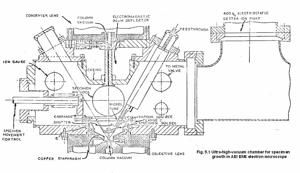
A second-hand commercial transmission electron microscope (AEI type EM 6) was purchased and the pressure in the specimen chamber was found to be about 2x10⁻⁴ Torr, but residual gas analysis with a mass spectrometer showed that a leak was present. A new contamination-free pumping system was fitted to the microscope, which enabled pressures of 1x10⁻⁶ Torr to be obtained in the pumping manifold. The specimen chamber was pumped by an electrostatic getter ion pump through a special-adaptor, and also reached a pressure of 1x10⁻⁶ Torr. Specimen contamination was greatly reduced, but not eliminated, since the
partial pressure of hydrocarbons (including methane) in the specimen chamber was 1x10⁻⁷ Torr.
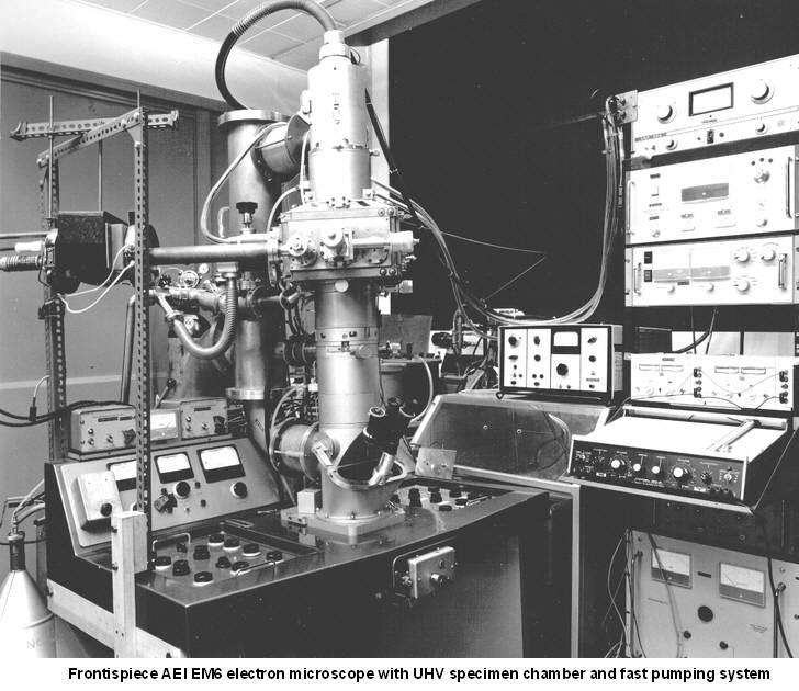
A new differentially pumped, stainless steel, metal sealed specimen chamber, originally designed by Grigson, was constructed, in which pressures of about 2x10⁻⁸ Torr (limited by leaks) could be obtained ([Tothill, Fig. 5.1] shows a modified later version). Unfortunately the pressure at the specimen was greater than 1x10⁻⁷ Torr, due to gas entering the chamber through the lower differential pumping aperture. The specimen contamination rate was less than 0.1 Å /minute. The [Tothill, Frontispiece] shows the modified EM6.
The control of the conditions of deposition during the in-situ preparation of evaporated films was poor, since it was not possible to alter the substrate temperature, the deposition rate was not accurately known, and it was not possible to prepare a clean substrate surface. A
resistively heated hairpin vapour source was used for the in-situ deposition of evaporated films, but the evaporation rate could not be calibrated, as it was not sufficiently constant. Silver, lead and gold were deposited by evaporation, onto carbon substrates at room temperature in the original specimen chamber but due to lack of time extensive experiments could not be performed. Islands of silver and gold started to coalesce before they were large enough to be resolved by the microscope, so no information was obtained on nucleation. Insufficient experiments were performed with lead to give useful results. Several deposits formed in the original specimen chamber were exposed to dry nitrogen at atmospheric pressure, and then re-examined: the coalescence effect for silver exposed to atmospheric pressure reported by Heritage was observed.
In a number of instances, islands coalesced between micrographs, or during the course of a series. "Liquid-like" coalescence, as reported by Pashley and Stowell (1966), was observed, although the coalescence and subsequent alteration in shape of the compound island was slower than in their experiments.
Tothill summed up:
“A considerable improvement in the vacuum performance of the new specimen chamber is possible without major modification. The reduction of the pressure in the objective lens gap would improve the pressure at the specimen by at least an order of magnitude (this has in fact been done by C.D. Bunting, who is continuing the work). The elimination of leaks in the "Beck" type metal seals, for example by the use of thicker gaskets or new flanges, should allow a pressure of at worst 2x10⁻⁹ Torr to be obtained in the chamber.
“Little can be done to improve the resolution limit of the microscope; modifications to the specimen movement might have some effect, but in view of the high level of ambient vibration at the site of the instrument, sophisticated anti-vibration mountings should be fitted.
“The initial experiments carried out so far have revealed two effects which require further investigation, namely the coalescence of islands, apparently without touching, and the effect of the electron beam. In the former case, it is important that the objective lens current is adjusted for true focus, rather than for maximum contrast, as the fringes which increase the contrast obscure details of low contrast, and impair the resolution. The variation of the effect of the electron beam with total current, current density, voltage and substrate material should
be studied. The possible contribution of the residual vacuum to the effect should also be considered.
“A differentially pumped specimen chamber capable of reaching ultra-high vacuum is one essential step towards controlling the environment of the specimen in the electron microscope. This is of importance in many other fields besides thin film deposition, such as the study at high temperatures of materials (such as silicon) which readily react with the residual gas under these conditions, low temperature studies, the investigation of oxidation and corrosion, catalysis, and the ob¬servation of biological specimens in a fully hydrated condition.
“With regard to the study of thin films, a quotation from the first paper describing in-situ deposition in an electron microscope, published 19 years ago, seems apposite: ‘It would appear that considerably more experimental information is required before a
quantitative theory of the mechanism of formation of evaporated films can be established’ (Sennett and McLauchlan, 1950).”
Tothill presented papers at two international conferences (Grigson et al., 1966; Tothill et al., 1968).
C. D. BUNTING
Christopher Bunting, having sat for the Natural Science Physics Part II Tripos in 1966 and the Electrical Sciences Tripos in 1967, took over the AEI EM6 electron microscope from Tothill in 1968. He also was supervised by Nixon.
The main aim of his research project was to convert the microscope for scanning microdiffraction and to use it in a study of the growth of thin, vapour-deposited metallic films grown in situ.
He set out to answer the following questions:
1. With what accuracy may the intensity and angle of the diffracted electrons be deduced from the traces?
2. What is the angular resolution?
3. What determines the recording time?
4. Over what time period are the conditions sufficiently stable to ensure reproducibility of measurements with specified precision?
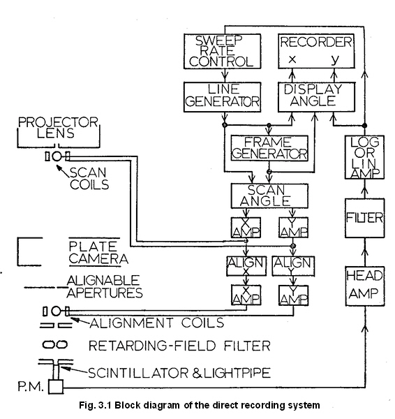
Bunting designed and built a new electronic system for deflecting the diffracted beams and detecting them with a scintillator and photomultiplier (see Block Diagram, [Bunting, Fig.3.1]). He investigated various plastic scintillators and selected Naton 11 (Everhart and Thornley, 1960) as having the best overall characteristics although its decay time was not the shortest. However since an X-Y pen recorder was to be used this was unimportant. The Naton conversion efficiency was also very uniform. In order to maximise the optical coupling efficiency between the Naton scintillator and the photomultiplier, no light guide was used. Instead, the scintillator was mounted to be in contact with the faceplate of the photomultiplier.
Electronic filtering of the photomultplier output was provided and this signal shaping minimised the distortion due to the limited writing speed of the pen recorder; the system was
tested by recording “two diffraction patterns of a gold film, the second ten minutes after the first. Intensities were equal within 1 per cent of full scale, and the peak positions were within 0.2 percent of full scale”.
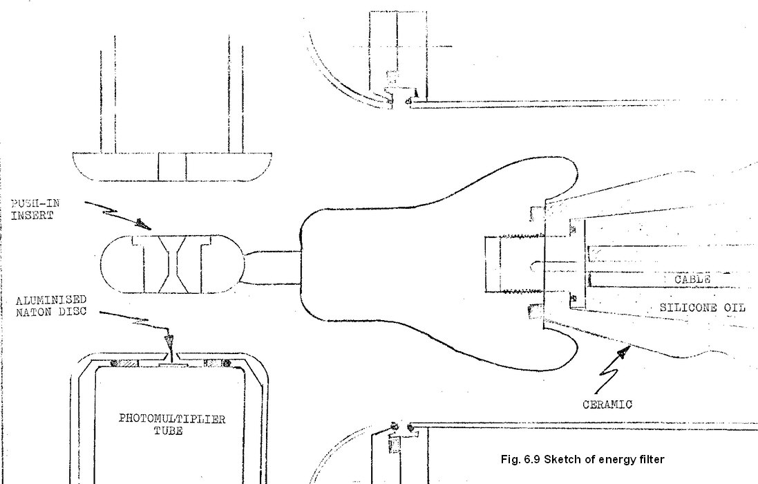
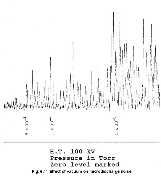
Bunting included an energy filter before the detector: he compared various designs (e.g. Denbigh, 1964; Grigson and Tillett, 1968) and made some alterations in the geometry of the electrodes “so as to be tolerant of greater angular misalignment than those designs where a more uniform retarding field has been deliberately engineered” [Bunting, Fig. 6.9]. There were difficulties with microdischarges that had been reported by other workers. These occurred when the vacuum pressure was lower than a critical pressure dependent on the operating voltage: typically 80 kV at 10-5 Torr, 90 kV at 8 x 10⁻⁵ Torr, and 100 kV at 5 x 10⁻⁴ Torr. The breakdowns were due to field emission from small protrusions on the surface of the negative electrode (Alpert et al. 1964) and caused an increase in the noise from the detector [Bunting, Fig. 6.11]. For this reason he had the filter at a pressure of 5 x 10⁻⁴ Torr: the high pressure would seem to preclude maintaining a very good vacuum in the specimen chamber (although < 10-8 Torr is mentioned) but this difficulty does not appear to be discussed.
Bunting shows a number of energy-filtered diffraction profiles together with images of evaporated or sublimed films on carbon substrates: e.g. [Bunting, Fig 8.1] for gold evaporated from a drop suspended on a molybdenum wire. Recording time per trace was about 10 sec and the deposition time between traces 90 sec. After each deposition the source was shuttered and a high magnification image was recorded.
REFERENCES
Bagdykyants, G.O., and Alekseev, A.G. (1958). Measurement of the scattered electron intensity and elimination of the background in electron diffraction studies. Bull. Acad. Sci. USSR Phys. Ser. 23, 766-768.
Bunting, C.D. (1971). ‘Scanning electron diffraction and transmission electron microscopy’ Ph.D. Dissertation, University of Cambridge.
Denbigh, P.N. (1964). ‘Scanning electron diffraction with energy analysis’ Ph.D. Dissertation, University of Cambridge.
Denbigh, P.N., and Dove, D.E. (1967). Scanning electron diffraction observations on diffuse rings from very thin vapor-deposited films. J. Appl. Phys., 38, 99-102.
Denbigh, P.N., and Grigson, C.W.B. (1965). Scanning electron diffraction with energy analysis. J. Sci. Instrum., 42, 305-311.
Denbigh, P.N., and Marcus, R.B. (1966). Structure of very thin tantalum and molybdenum films. J. Appl. Phys. 37, 4325-4330.
Dove, D.B., and Denbigh, P.N. (1966). Modified detector arrangement for scanning electron diffraction instrument. Rev. Sci. Instrum. 37, 1687-1689.
Dove, D.B., Grigson, C.W.B., and Stilwell, G.R. (1964), 3rd Europ. Conf. Electron
Microscopy, Prague, p. 399.
Grigson, C.W.B. (1955). ‘An electron diffraction study on the growth of ionic crystals’. Ph.D. Dissertation, University of Cambridge.
Grigson, C.W.B. (1961). High-speed direct recording system for electron diffraction. Nature (London) 192, 647-648.
Grigson, C.W.B. (1962). On scanning electron diffraction I. J. Electron Control 12, 209-232.
Grigson, C.W.B. (1965). Improved scanning electron diffraction system. Rev. Sci. Instrum.
36, 1587-1593.
Grigson, C.W.B. (1966). Scanning electron-diffraction studies of nucleating films. J. Phys. Chem. Solids Supplement 1.
Grigson, C.W.B. (1967). Validity of the Debye scattering equation in elastic electron diffraction. Nature (London) 215, 382-383.
Grigson, C.W.B. (1968). Studies of thin polycrystalline films by electron beams. Adv. Electron. Electron Phys. (Supplement 4), 187-289.
Grigson, C.W.B., and Barton, E. (1967). The development of face-centered cubic interference function as crystals grow. Brit. J. Appl. Phys. 18, 175-183.
Grigson, C.W.B., and Dove, D.B. (1966). Scanning electron diffraction of film growth. J. Vac. Sci. Tech., 3, 120-132.
Grigson, C.B.W., Dove, D.B., and Stilwell, G.R. (1964). Amorphous magnetic films.
Nature (London) 203, 173.
Grigson, C.W.B., Dove, D.B., and Stilwell, G.R. (1965). Some applications of an improved scanning electron diffraction system. Nature (London) 205, 1198-1199.
Grigson, C.W.B., Heritage, M.B., and Tompsett, M.F., (1966). Intensities in filtered and unfiltered electron diffraction from thin films. Nature ( London) 212, 390-391.
Grigson, C.W.B., Nixon, W.C. and Tothill, F.C.S.M., (1966). Sixth International Congress for Electron Microscopy, Kyoto, p. 157.
Grigson, C.W.B., and Tillett, P. I. (1967). Filtered electron diffraction measurements from thick polycrystalline metal foils. Nature ( London) 215, 617-618.
Grigson, C.W.B. and Tillett, P.I. (1968). On scanning electron diffraction II. Int. J. Electronics 24, 101-138.
Grigson, C.W.B., and Tompsett, M. F. (1966). Determination of radial distribution functions by elastic electron diffraction. Nature ( London) 210, 86-87.
Heritage, M.B. (1968). ‘Growth studies on thin films using scanning electron diffraction’. Ph.D. Dissertation, University of Cambridge.
McMullan, D. (2004). Scanning electron diffraction: a survey of the work of C.W.B. Grigson. In ‘Charles Oatley and the Scanning Electron Microscope’, B. Breton, D. McMullan and K.C.A. Smith, eds., Adv. Imaging & Electron Phys. 133, 227-233.
Pashley, D.W., and Stowell, M.J. (1966). J. Vac. Sci. Tech. 3, 156.
Sennett, R.S. and McLauchlan, T.A. (1950). J. Appl. Phys. 21, 72.
Tillett, P.I. (1969). ‘Scanning electron diffraction at cryogenic temperatures’. Ph.D. Dissertation, University of Cambridge.
Tillett, P.I., and Grigson, C.W.B. (1967). Reflexion scanning electron diffraction from growing films. Nature ( London) 214, 77-78.
Tompsett, M.F. (1965). ‘Reflection scanning electron diffraction with energy analysis’. Ph.D. Dissertation, University of Cambridge.
Tompsett, M. F., and Grigson, C.W.B. (1965). Scanning electron diffraction from solids. Nature (London) 206, 923-924.
Tompsett, M. F., and Grigson, C.W.B. (1966). Reflection scanning electron diffraction with energy filtering. J. Sci. Instrum. 43, 430-435.
Tompsett, M. F., Heritage, M. B., and Grigson, C.W.B. (1967). Small-angle filtered electron diffraction from growing films. Nature (London) 215, 498-499.
Tothill, F.C.S.M. (1969). ‘Ultra-high vacuum in a transmission electron microscope for observing thin film growth’. Ph.D. Dissertation, University of Cambridge.
Tothill, F.C.S.M, Nixon, W.C., and Grigson, C.B.W., (1968). Fourth Regional Conference on Electron Microscopy, Rome, p.229.