IV. RESEARCH DIRECTED BY
K. C. A. SMITH
B. Computational and Experimental Electron Optics
C. Image Storage and Processing
In their seminal paper on the SEM Zworykin, Hillier and Snyder (1942) refer to their attempt at utilising field emission: “The principal problems encountered in the design of an electron scanning microscope are concerned with resolution and intensity…… A first attempt to overcome this difficulty by making use of the much higher current densities obtainable with field emission cathodes yielded promising results, but was abandoned in view of the unsteadiness of cathodes of this type.” After this first attempt, another two decades were to elapse before the problem of ‘unsteadiness’ was to a significant degree overcome by Albert Crewe who in the late 1960s was reporting good results with his field emission gun (Crewe et al 1968). There was therefore reason to believe that the application of field emission to the kind of SEM developed in the CUED offered a viable project for a PhD research student. The Department at that time had little experience of UHV systems of the type requisite for field emission cathodes, and the project initially necessitated the acquisition of expertise in several new areas, in particular the fabrication and welding of stainless steel components.
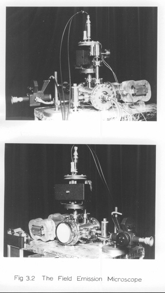
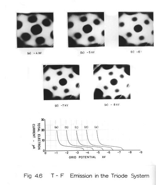
The primary aim of the project was to establish the factors affecting the lifetime and stability of the emission current from various types of emitter. A second objective was to explore the electron optical characteristics of systems employing field emission guns. The first phase of the work involved the construction of a field-emission microscope to observe the emission patterns from both cold-field and TF emitters under various operating conditions. This task fell, in 1966, to the first research student on the project, David Swann , who was required to master a whole range of techniques new to the laboratory involving the preparation of tungsten single-crystal emitters, their mounting on hairpin filaments and the flashing procedures required for stable operation. Construction and operation of this microscope enabled all of the operational requirements of UHV – bakeout cycles, residual gas analysis etc. – to be established.
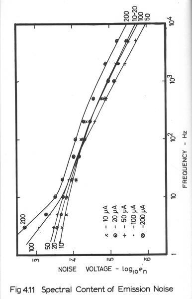
The microscope and some of the patterns obtained with it are shown in [Swann, Fig. 3.2] and [Swann, Fig. 4.6] (Swann 1971). The low-frequency stability of the emitted current was monitored on a pen recorder, and for the higher frequency (noise) components the light output from the phosphor screen was observed by means of a photomultiplier coupled to a wave analyser. By masking off all but a delineated area of the screen it was possible to select the light output from different regions of the emission pattern corresponding to different crystal faces at the tip. A typical noise spectrum is shown in [Swann, Fig. 4.11]. The microscope was used also to investigate emitter lifetimes as a function of pressure and other parameters. The introduction of a control electrode enabled experiments to be conducted under pulsed emission conditions.
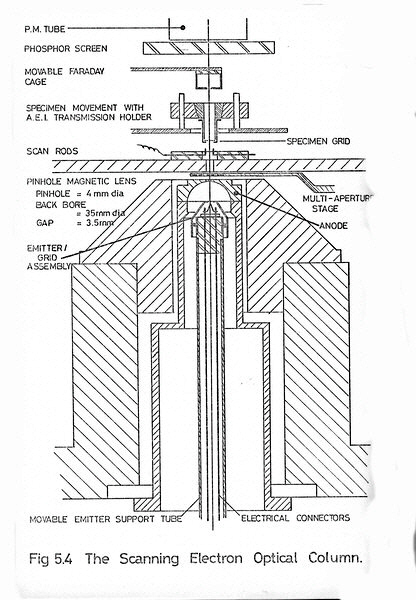
In the second phase of the research Swann constructed a complete single-lens SEM. The emitter assembly was mounted in a differentially pumped chamber with the emitter located in the back bore of the magnetic lens. The design of a satisfactory mechanism for aligning the emitter with the aperture and both with the optical axis of the lens – all operating at UHV – was a very considerable achievement. A diagram of the gun and lens assembly is shown in [Swann, Fig. 5.4]. With this apparatus Swann was able to measure scanning spot size, beam brightness and other parameters. Some preliminary work on pulsed operation of the microscope was also undertaken.
After completing his work at the Engineering Department, Swann went to the CIC where he, in collaboration with David Kynaston, Technical Director of the Company, built a field emission SEM with a view to placing it on the commercial market (Swann and Kynaston 1973). This prototype was demonstrated at a commercial exhibition, but the project proved to be altogether too ambitious for the resources available to the Company and was eventually terminated. It can, however, be recorded as the first commercial venture for this type of microscope in the UK.
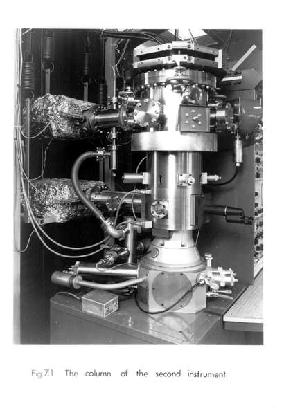
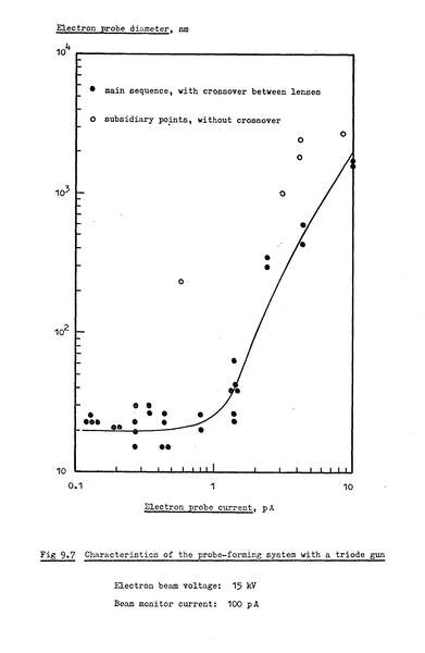
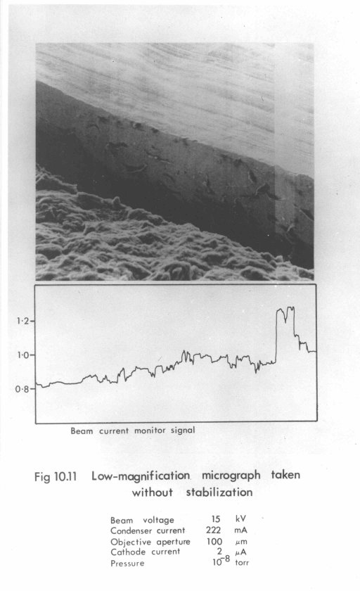
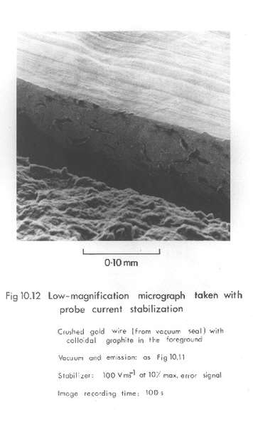
The results obtained by Swann were considered to be sufficiently encouraging to warrant further research, and a second student, John Cleaver, was engaged in 1969 to continue the work. His main task was to adapt a Stereoscan Mark 2A (generously made available by CIC) for field emission operation. This entailed replacing most of the electron optical column, except for the final scanning objective lens, with a differentially pumped UHV system. With this instrument he was able to determine the optical characteristics and performance of complete probe-forming systems operating with both triode and tetrode field emission guns. [Cleaver, Fig. 7.1] (Cleaver 1973) is a photograph of the modified microscope column, and [Cleaver, Fig. 9.7] shows measured probe current versus probe diameter for a system with a triode gun. A system for electronically stabilising the current in the electron probe to compensate for changes in cathode surface properties was also constructed. [Cleaver, Fig. 10.11] and [Cleaver, Fig. 10.12] compare micrographs taken with and without stabilisation, which show that the system worked well at low magnification, but subsequent experiments revealed the limitations of this approach at high magnification.
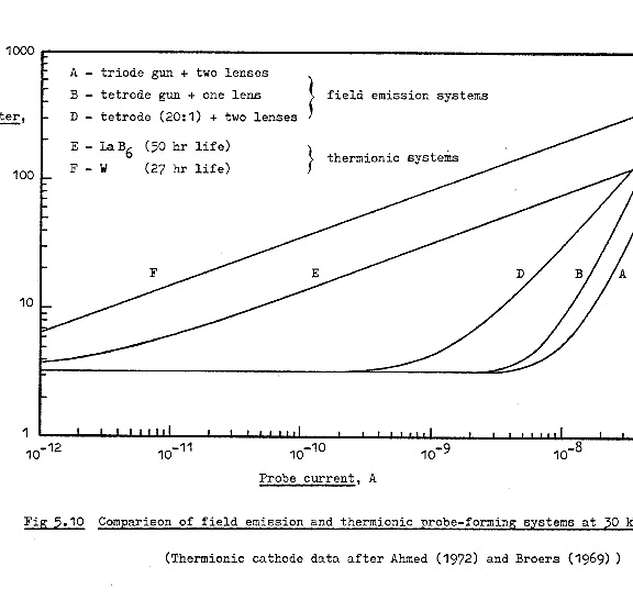
This practical work was complemented by a theoretical and computational study, which took into account aberrations arising in both gun and lenses. The optical characteristics of several different electron guns incorporating field emission cathodes were computed, and the first-order properties and the principal aberrations were then combined with magnetic lens characteristics to predict the properties of complete systems. Part of the analysis utilised the finite element technique introduced by Munro (1971). The results of these computations are summarised in [Cleaver,Fig.5.10]. They predict that a system equipped with a field emission gun, operating at the optimum resolution determined by spherical aberration and diffraction of the final lens, should give a probe current about a hundred times that of a system with a lanthanum hexaboride gun.
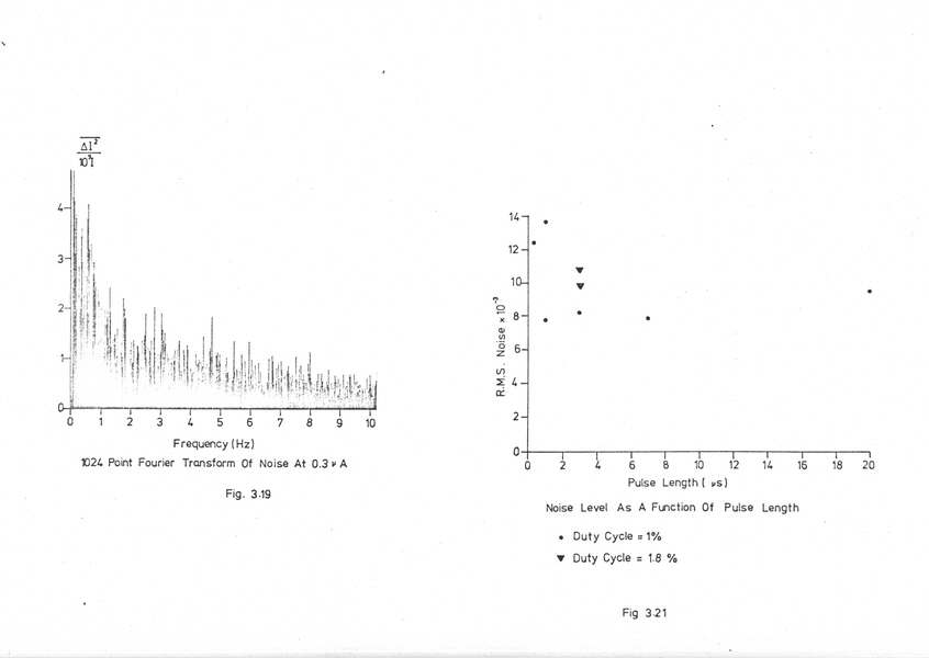
The research was continued in 1974 by Duncan Cumming who investigated two specific problems relating to the application of field emission cathodes to the SEM: fluctuations of the emission current and energy broadening of the emitted electron beam. Swann’s work had revealed that low-frequency fluctuations in the range 0-10 Hz were of major importance. Cumming refined the method developed by Swann by coupling the screen of the field emission microscope to the photomultiplier via a flexible fibre-optic light pipe, which enabled him to select and measure the noise corresponding to any area of the emission pattern. The output signal from the photomultiplier was fed to a specially constructed true RMS noise meter. A spectral analysis of the noise signal was carried out using a minicomputer for which special software had to be developed at the time. An early result obtained with this system is shown in [Cumming, Fig. 3.20] (Cumming, 1978).
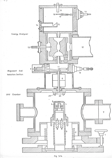
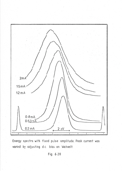
The other major project undertaken by Cumming was the construction of an energy analysing column with which to measure energy spreads in the emitted electrons as a function of total current. A cross-section of the column is shown in [Cumming, Fig. 5.14]. The analyser is of a type due to Brack (1962), which consists of an einzel lens with a superimposed axial magnetic field. In order to make measurements over a very wide current range, the system was designed to operate in a pulsed mode, which allowed peak currents of up to 2 mA to be drawn from cathodes whilst retaining reasonable emitter lifetimes. Energy spectra for a current range 0.2-2.0 mA are shown in [Cumming, Fig. 6.20]. The energy spread broadens with increasing total emission current, rising to 3.8 eV FWHM at 2.0 mA. In the course of his work Cumming also developed an ingenious computer method for reconstructing the three dimensional shape of a field emitter from multiple shadow profiles taken in the TEM.
In 1972 Professor Tom Mulvey patented his single-pole magnetic lens (UK patent No. 1395201) and it occurred to both Cleaver and Smith that this lens might have application to the field emission gun. The novel configuration they proposed is shown in a CUED Report by Smith (1977) [Smith, Fig. 2]. (See also Cleaver, 1979, 1980.) At the same time interest was growing in Munro’s finite element method for the design of electron optical systems, and funds were subsequently obtained to undertake a computational study of this gun configuration. Andrew Stokes, a post-doctoral student who had worked with Professors E. J. Davies and Tom Mulvey in the Electrical Engineering Department at Aston University (Stokes, 1978), was engaged to undertake this work. Experimental work on this system was also begun, which proceeded intermittently until 1987 when the project was terminated inconclusively with Smith’s retirement. The work, however, initiated the extensive program of general computational design studies described below.
B.Computational and Experimental Electron Optics
The introduction by Munro of the finite element technique (see section VII) opened a new era in the design of electron optical systems. The ability to handle saturated magnetic lenses of unconventional shapes allowed the designer free play to explore new and original magnetic circuit and coil configurations. Munro (1975) published the complete FORTRAN code and made it available on the University IBM 370 mainframe computer, with precise instructions for its use. It was possible therefore for relatively inexperienced users to try out their own electron optical ideas.
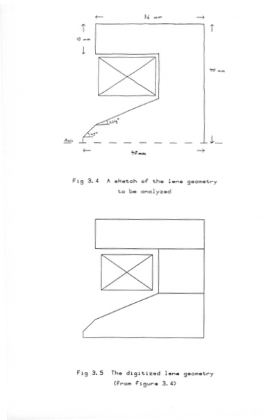
The single-pole lens of Mulvey appeared to be an ideal application for this new technique, and it was decided to explore the possibilities of using such a lens in the SEM. This project was assigned to Raymond Hill who began his PhD research in 1977. Initially he used the Munro program suite available on the University mainframe to carry out a preliminary study, but it quickly became evident that the limitations imposed by working on the IBM 370 – batch-mode submission of jobs, long turn-round times, and restrictions on the number of finite element mesh points the machine could handle – seriously hampered the kind of design work envisaged. Experience showed also that construction and entry of the data tables required to provide information about the lens under investigation was time consuming, required great care, was prone to error and could lead to excessive amounts of time spent in re-running jobs submitted. Typically two days would be required to produce results for a single design.
Hill therefore decided to adopt a completely different approach: the Munro programs were rewritten to run on an available local laboratory minicomputer, and a new system of interactive working devised. A key element of this system was a four-pen digitising plotter, which could be used for both input and output of data. With this new system it was only necessary to place a sketch of the proposed lens on the plotter, use the digitising sight to define salient points of iron circuit and coils and areas for mesh generation etc., and the computer would deliver a digitised version of the lens together with graphs of flux density distribution, tables of optical properties and other relevant data. [Hill, Fig 3.4-5] (Hill, 1982) illustrate the initial stages of the interactive design procedure. Although execution time on the mini computer was much slower than that on the mainframe, the actual turn-round time for a job was far less. As many as eight variants on a design could easily be obtained in a normal working day. Hill made a further advance with his introduction of a finite element mesh distribution laid out according to a geometric law. By this means it is possible to have a very fine mesh spacing in regions where high accuracy is required, while at the same time achieving a smooth transition from fine to coarse spacing, thus avoiding errors induced by discontinuities.
The system as devised by Hill and later extended by Taylor (see below) was dubbed CIELAS – Cambridge Interactive Electron Lens Analysis System. The program was later transferred to CIC where Dr Julian Davey, formerly a member of Cosslett’s Group in the Cavendish, adapted it to run on a VAX computer, and used it with considerable effect in the work of the Company. As part of a design study undertaken on behalf of CIC, the CIELAS program was used by Smith and Breton to evaluate the characteristics of a special multi-coil lens having an extended axial field distribution, particularly favourable for achieving a low spherical aberration coefficient at long working distances. An experimental version of the lens with the best computed characteristics was constructed and evaluated using a shadow projection method.
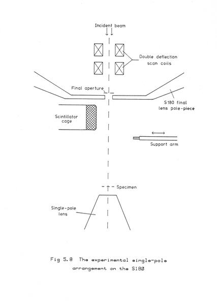
Hill’s experimental work on the single-pole lens was carried out on a Cambridge Stereoscan S180 SEM generously loaned to the Department by CIC. The primary aim was to establish the feasibility or otherwise of using such a lens as a post-specimen scanning objective. A schematic of the experimental arrangement is shown in [Hill, Fig. 5.8]. The miniature experimental lens was mounted in the specimen chamber of the microscope on a stripped-down specimen stage so that the lens could be aligned with the axis of the column by means of the X-Y movements of the stage. A simple specimen stage was built operated through one of the auxiliary ports in the chamber, and the normal S180 microscope aperture was used as the beam-defining aperture for the single-pole lens. Scanning was effected using the normal scan coils.
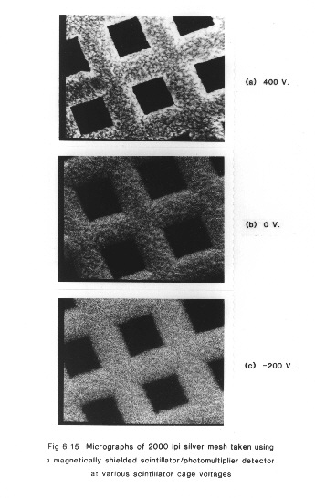
The major difficulty in using the single-pole lens as a scanning objective lies in the efficient collection of the secondary electrons since the low energy electrons follow paths that spiral tightly round the magnetic field lines, and the back scattered electrons are constrained close to the axis of the lens. Experiments were conducted to determine the secondary electron distribution in the lens/specimen region, and various detector schemes were explored including solar cell, biased plate, and conventional scintillator/photomultiplier detectors. [Hill, Fig. 6.15] shows images of a silver grid test specimen obtained with a scintillator/photomultiplier detector. The collection efficiency of all of the detector arrangements tested were, however, relatively poor, and it was concluded that if advantage of the favourable aberration coefficients and other features of this type of lens were to be realised a much improved detector system would have to be developed.
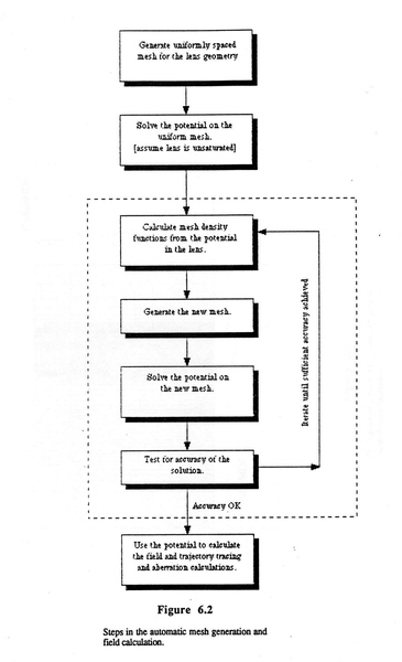
Development of the finite element method in electron optics was continued in 1987 by James Taylor who undertook a detailed examination of the errors arising in the various steps in the procedure, particularly in connection with layout of the finite element mesh. In the original Munro programs and in the CIELAS program developed by Hill, the user laid out the mesh, literally by eye, to produce, in the light of experience, a satisfactory distribution of elements. Such a procedure could lead to large errors in the calculated lens properties. Taylor developed measures of error that indicated the accuracy of the solution and developed techniques to reduce or eliminate interpolation and boundary errors. This work culminated in the creation of a completely automatic method of mesh generation.
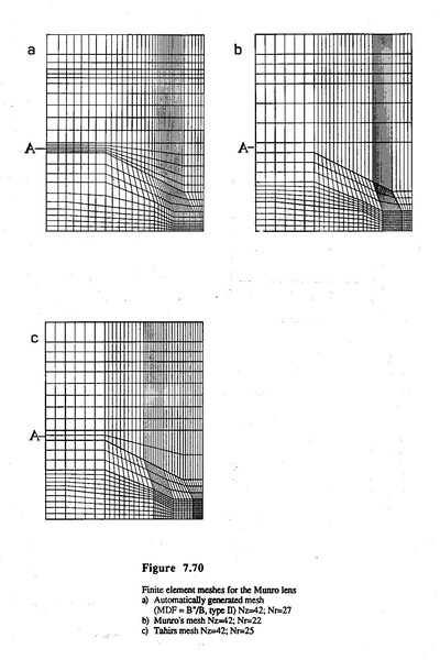
Steps in the automatic procedure are outlined in the flow chart of [Taylor, Fig. 6.2] (Taylor, 1990). The process begins, after the geometry of the lens is defined, by obtaining a crude field solution using a uniformly spaced mesh. From this ‘mesh density functions’ (dissertation, page 39) are derived from which a more accurate mesh is calculated. An iterative procedure is then followed until an appropriate test for accuracy of the field solution is satisfied. Development of the automatic mesh generator enabled a great variety of numerical experiments to be undertaken on various types of lens including saturated high-resolution, SEM conical (snout), and single pole lenses. A comparison of mesh layouts for a test lens investigated by Munro [Taylor, Fig. 7.70] showed that the auto mesh generator gave substantially greater accuracy in the computed lens properties.
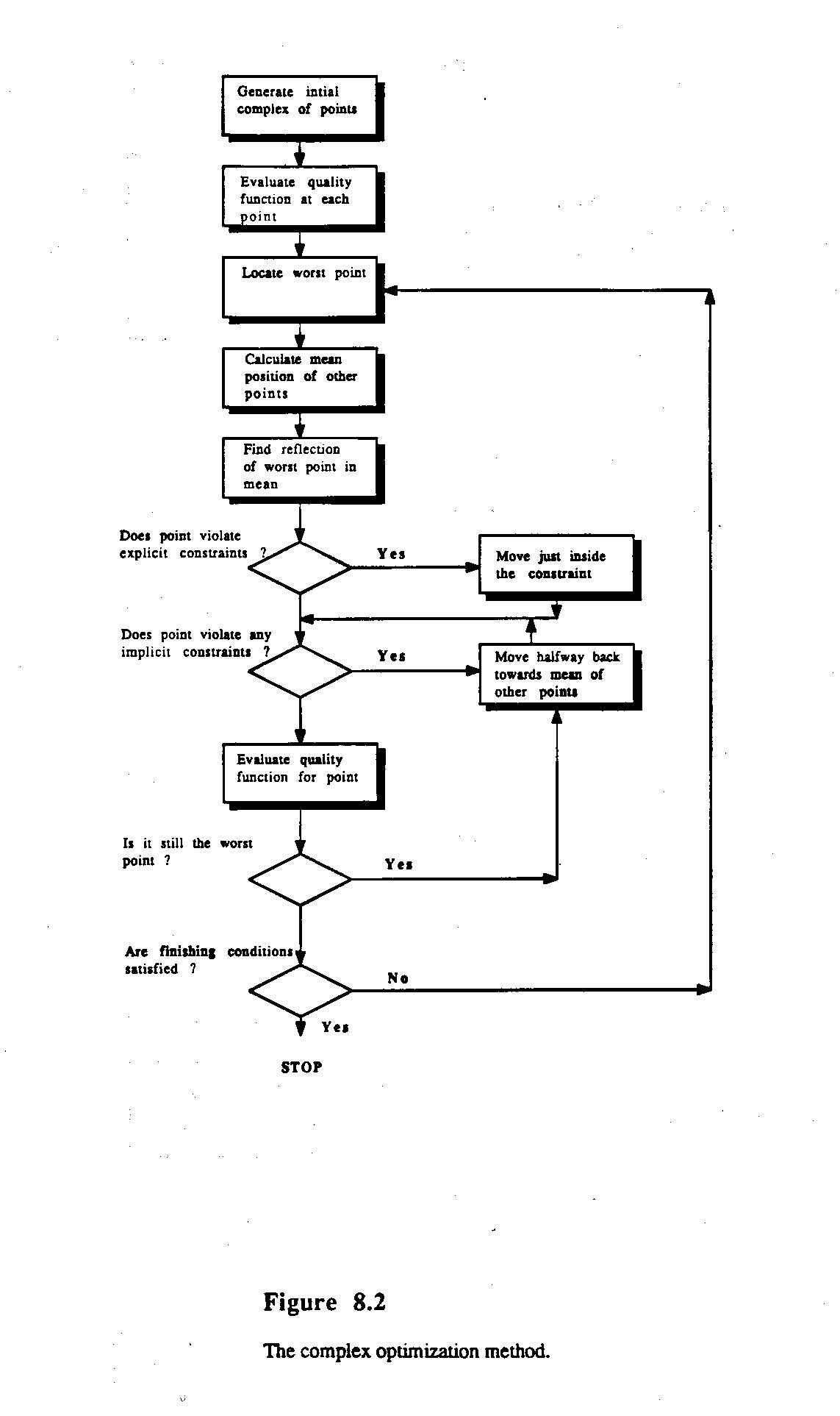
The final part of Taylor’s work was concerned with the problem of lens optimisation. The procedure he developed was based on the complex method illustrated in [Taylor, Fig. 8.2]. In this method a set of points in N-dimensional space, each point representing a lens geometry, are manipulated until the figure described by the points collapses towards a single point, which is the minimum. A particular advantage of the complex method is that the distribution of points in the complex at the end of the optimization gives an idea of how successful it has been, and can indicate if there is more than one minimum. The constraints of the problem are also dealt with easily. For these reasons the complex method is probably the most suitable for electron optical problems.
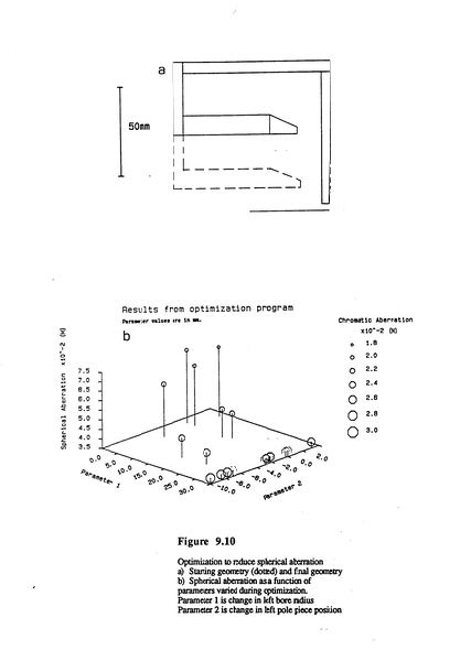
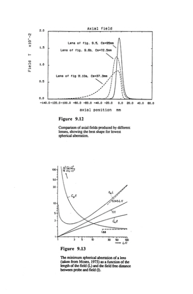
Using the optimisation program a wide variety of lens types was investigated. These included the standard lens used in the CUED for teaching purposes, a high-resolution TEM objective lens, a double-gap lens, and a single-pole lens. The factors affecting lens performance - gap, front and back bore diameters, pole-piece shape, thickness of the iron circuit and the size of the lens - were determined, and several measures of performance analysed, such as the spherical aberration, the chromatic aberration, and the minimum spot size in a probe forming system. In addition to finding the best lens within a given set of constrains, the optimisation program also allowed the designer to deduce rules about how the geometry of a lens affects the aberrations. [Taylor, Fig. 9.10], for example, shows an optimisation aimed to reduce spherical aberration, which also shows how the chromatic aberration increases in the process. [Taylor, Fig 9.12] compares axial fields produced by different lens geometries, showing the best shape for lowest spherical aberration.
Taylor's optimisation program incorporating automatic meshing represented a significant advance in the application of the finite element method to electron optical problems. On completion of his PhD work in 1987, Taylor moved to CIC where he continued to play a leading role in the development of the SEM. His departure marked the end of this line of research and development in the Department.
The work of Stokes, mentioned above, and the realisation that space charge effects were important in high-current field emitters, led to an extension of the interactive computational work to cover space-charge limited systems of all types. Funds were obtained to replace the original minicomputer with a more powerful computer and to employ a succession of post doctoral research workers to follow Stokes. Major support for the project was obtained from the Royal Aircraft Establishment, Farnborough. Those participating in this project included Tim Smith, Derek Roberts (both formerly PhD students with Peter Spreadbury) and Christopher Edgcombe who was formerly with Professor Bill Beck. John Banbury of the RAE (formerly with Bill Nixon) was also an active participant. The end result of the project was a finite element computer program called CIELAS2. In 1987 a company, Granta Electronics Ltd., was formed by three of those involved – Edgcombe, Roberts and Smith – to exploit the program commercially through the auspices of the British Technology Group. By 1995 the software suite, running on a standard PC, provided interactive graphical specification of geometry, solution for electric and magnetic potentials and fields, tracing of particle trajectories, iterative current estimation, modelling of the full range from thermionic to field emission, calculation of spherical and chromatic aberration, brightness, emittance, perturbation of electrodes, autofocus and many other facilities. Several research groups and manufacturers of electron optical devices have used the program, mainly for the design of miniature cathode-ray tubes, microwave tubes and electron beam welders.
C. Image Storage and Processing
An essential element in the success of McMullan’s first SEM was the incorporation of a radar-type cathode-ray tube for visual observation of the image. The long persistence screen of this tube gave an integration time of a few seconds, sufficient to reduce noise to an acceptable visual level, and it enabled the operator, albeit with some difficulty, to focus and correct astigmatism. But the distracting nature of the slow-scan and lack of flexibility imposed severe limitations on the general convenience of operation of the instrument. In the late 1960s analogue storage tubes became available at reasonable cost, and appeared to offer considerable advantages in terms of flexibility and convenience for display of the SEM image. A research project was therefore initiated to assess the capabilities of the various types of tube on the market and to construct an experimental system for use with the SEM.
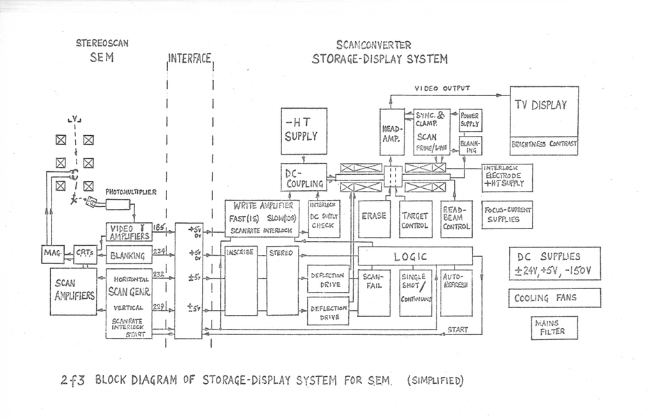
In 1968 John Catto commenced work on the project, and after an initial assessment, decided to investigate the potential of a scan-converter tube manufactured by a local Cambridge company, Cathodeon Ltd. In this type of tube a signal, in this case from the SEM, modulates a writing beam which is scanned in synchronism with the SEM. This deposits a charge pattern on a fine mesh coated with a layer of insulating material. A second, very fine beam is scanned in a TV raster across the storage mesh and is modulated by the stored charge. The resulting signal is collected on a second mesh coupled to a high-gain video amplifier. This signal is then used to drive a standard TV monitor.
A block diagram of the storage-display system developed by Catto is shown in [Catto, Fig. 2f3] (Catto, 1971). An important feature of the system is the logic circuitry which monitors the SEM scanning circuits and which blanks the write gun or switches off the HT if the scan fails for any reason or if the microscope is switched to ‘spot’. This protection is necessary because a beam remaining stationary on the storage mesh will destroy the tube.
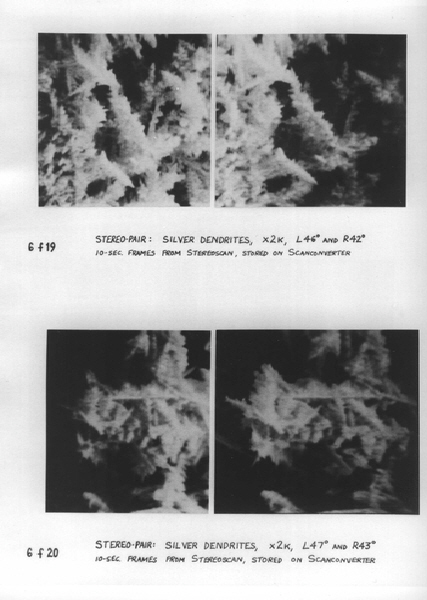
Special electronic equipment to test the scan-converter system had to be constructed, e.g. star and bar pattern generators, to measure distortion and shading. The system was found to be capable of resolving almost 400 lines and about 10 grey levels. Images could be stored and displayed for five minutes without too much deterioration in quality. An example of a stored stereo pair is shown in [Catto, Fig. 6f19]. A viewing hood incorporating an optical system was constructed to facilitate the observation of such pairs.
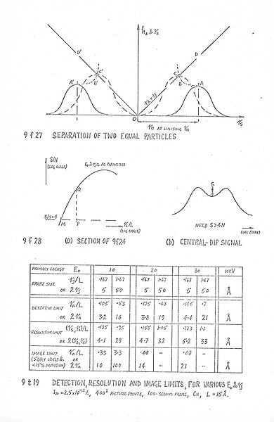
For the final part of his PhD work Catto turned his attention to the ultimate topographical detection and resolution limits of the SEM operating with a field emission gun. The model he considered for the beam-specimen interaction is illustrated in [Catto, Fig. 9f1]. It consists of a small asperity modelled with a gaussian profile, situated on the flat surface of the specimen, the beam being incident normal to the specimen surface. It is assumed that the specimen is of copper and that it is a homogeneous, isotropic solid. All the secondaries emitted are assumed to be collected by an ideal, noise-free detector.
Using this simplified model, the contributions to the total secondary electron signal - that arising from the particle, that generated by the primary beam within the specimen, and that generated by backscattered electrons emerging from the surface of the specimen – were calculated, and from signal-to-noise ratio considerations, an estimate was obtained for the size of asperity detectable. An extension of the theory allowed an estimate to be made of the resolution limit.
The calculations were performed for an infinitely thin beam, and for beam diameters of 0.5 and 5.0 nm, and for three different accelerating voltages: 10, 20, and 30 kV. The results of the calculations are summarised in [Catto, Fig. 9t19]. For 0.5 and 5.0 nm beam diameters the corresponding figures for the resolution limit are 0.41 and 2.9 nm respectively at 10 kV.
Catto concludes that these figures must be interpreted with due regard to the approximate nature of the theory and experimental inaccuracies in some of the important physical quantities involved. Furthermore, the assumption that the normal secondary emission theory, valid for large surface areas and volumes of material, is also valid for small asperities approaching lattice dimensions, must be questioned. Nevertheless, the theory does indicate that secondary electron diffusion effects may not be as important as hitherto supposed in limiting resolution and that, with the fine electron beams potentially available with a field emission gun, topographic detail at the one nanometre level might be resolvable on a metallic specimen.
About the time Catto was completing his work, in the early 1970s, the storage and manipulation of images in the digital computer was becoming well established; moreover, minicomputers were becoming increasingly available at reasonable cost. It was evident that digital computer techniques would have applications in the field of scanning electron microscopy. In 1972 Brian Unitt commenced his PhD work on the topic of on-line digital image processing for the SEM. As a preliminary, and before investing in on-line equipment, it was decided to obtain some experience in image processing using the newly-installed IBM 360 mainframe computer purchased by the University. (This system suffered many teething troubles, and much time was wasted as a result.)
For this preliminary work scanning micrographs, in the form of transparencies, were digitised using a Joyce-Loebl Scandig microdensitometer. (This instrument was used with the kind permission and help of Dr Peter Hawkes, then working in Cosslett's Group in the Cavendish Laboratory.) Data from the microdensitometer was transferred to the IBM 370 by means of magnetic tape.
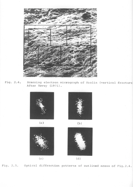
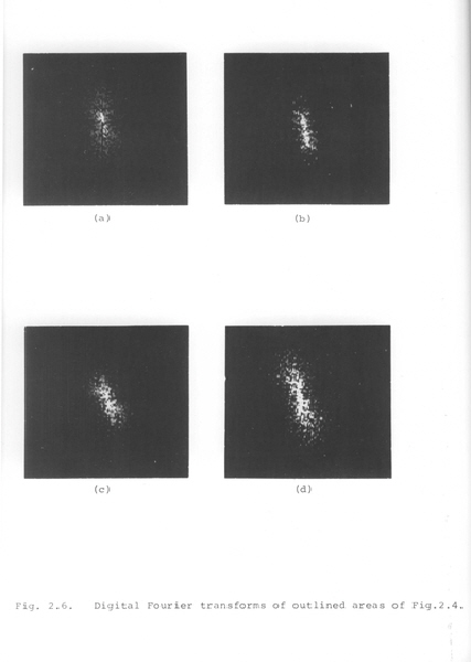
One of the first off-line investigations was undertaken in collaboration with Dr Keith Tovey who was then working in the Soil Mechanics group in the Department. He was studying the orientation of particles in samples of soil using the SEM in conjunction with an optical diffractometer. The initial experiments were carried out simply to ascertain whether Tovey's results could be reproduced by means of two-dimensional Fourier transforms calculated with the IBM 370. The main difficulty encountered in this work was displaying, with the equipment then available, the computed Fourier transforms in a way that would allow direct comparison with photographs obtained by means of the optical diffractometer. The most effective method was found to be by transferring the data from the IBM 370 to a small Nova 820 computer (used with kind permission of Professor Peter Brandon) equipped with a CRT display, which could then be photographed. Transfer of data to the Nova was, however, extremely cumbersome requiring 40 metres of punched paper tape for each 128-line image; consequently, most of the experimental work was performed using a line-printer programmed to produce, by means of overprinted characters, a crude grey-scale image. [Unitt, Fig. 2.4] and [Unitt, Fig. 2.5] Unitt (1976) show respectively a surface of kaolin and its corresponding optical diffraction patterns, while [Unitt, Fig. 2.6] shows the equivalent digital Fourier transforms. In this initial phase several potential applications of image processing for the SEM were explored including an investigation of the Walsh and Hadamard transforms. The experience gained proved invaluable when proceeding to the design of the on-line system.
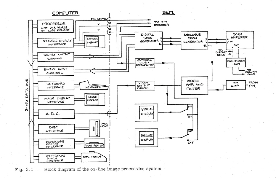
In the early 1970s no existing minicomputer of reasonable cost contained sufficient storage capacity and speed to process images at the full line a resolution of which the SEM was capable; therefore, two basic modes of operation for the on-line system were proposed. First, storage and processing at a limited line resolution; second, a serial mode in which the computer accepts the video signal from the SEM, processes the information and returns the resulting signal to the SEM for display and photography in the normal fashion.
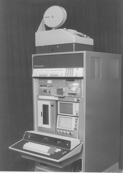
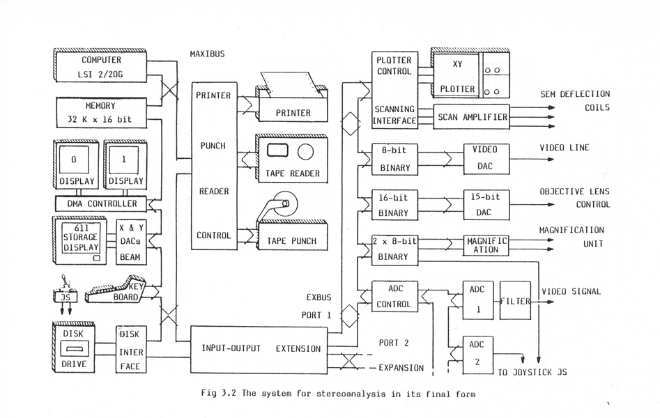
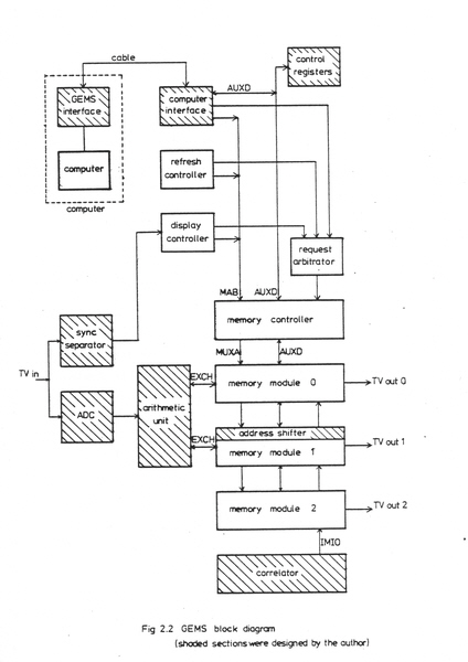
A block diagram of the system designed by Unitt is shown in [Unitt, Fig. 3.1]. The minicomputer is a 16-bit Computer Automation Alfa LSI 2 containing 24 K of core memory, sufficient to store two 128-line (128x128 pixel, 8 bit) images. This was the only low-cost minicomputer then available with an output data rate sufficiently great to transfer images to a raster scanned display. For the display itself a standard laboratory oscilloscope was utilised. Backing storage was provided by a floppy disk system with a capacity of 300 KB per disc, capable of holding about twenty 128-line images. The complete system, costing about £5,000, is shown in [Unitt, Frontispiece]. To complement the system Unitt constructed a digital scan generator capable of producing a variety of different raster formats, including a square spiral scan.
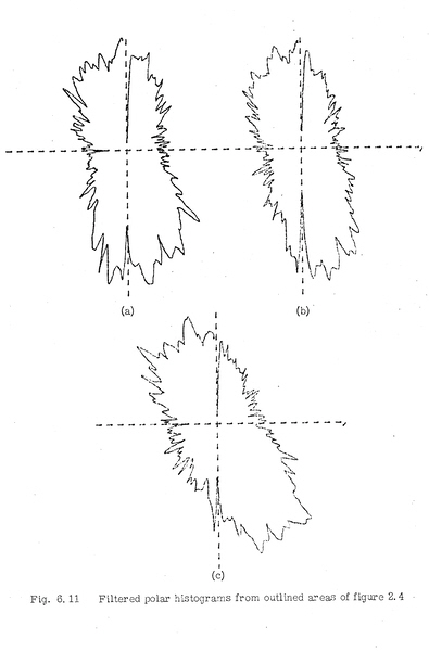
Although rudimentary by today's standards, the system allowed a great variety of image-processing techniques to be explored. Software was written to simulate all the usual analogue processes available on the SEM, such as contrast expansion and gamma correction. In the storage mode processing operations involving Fourier transforms became available and, with two images buffers, quantitative measurements on stored stereo pairs were feasible for the first time. True gradient processing, not possible with analogue circuitry, proved to be a particularly fruitful line of investigation. In a continuation of the off-line work on orientation analysis of particles in soil samples, a method was devised by Unitt to utilise the gradient image to detect orientation. His results were presented in the form of a polar histogram, which represented graphically the overall orientation within a sample in a fashion somewhat similar to the Fourier transform. [Unitt, Fig. 6.11] shows polar histograms obtained from the kaolin sample of [Unitt, Fig. 2.4], which should be compared with the optical diffraction patterns and Fourier transforms of [Unitt, Fig. 2.5] and [Unitt, Fig. 2.6].