Research
Selected recent research themes
Nano-manufacturing the materials of tomorrow
The ability to engineer device materials at a sub-100nm scale opens unmatched opportunities to tailor enhanced electrical, optical, magnetic and mechanical properties and functionalities that can be effectively integrated and combined into new form factors and technologies. Inasmuch as integrated circuits and systems shaped our society over the last decades, integrated nanomaterials are set to have revolutionary impact on an ever increasing number of sectors, including information & communication technologies, healthcare, energy conversion and storage, security, transport and environmental technologies. With the size of materials reduced to nm-size scale, their properties not only depend ever more closely on their detailed structure, size, shape and dimensionality but importantly also on their surfaces and interfaces. Much of the new functionality arises from the ability to combine an increasing diversity of materials and achieve greater structural complexity and more complex device architectures. This necessitates new growth and heterogeneous material integration strategies, and for nanomaterials bottom-up or self-assembly approaches are thereby of crucial importance. We investigate crystal growth of nanomaterials that is at the heart of all such emerging technology and is the key future enabler.![]() Semiconducting Nanowires
Semiconducting Nanowires
We explore catalytic growth, self-catalysed growth and selective area epitaxy. Large local supersaturations open many new kinetic pathways, which leads to striking new crystal growth behaviour on the nanoscale and makes this an extremely exciting field of study. We study phase behaviour of nano-scale alloys, the atomistic dynamics of nano-crystal nucleation and dynamics at liquid-solid, solid-gas and solid-solid interfaces in realistic process environments. Such fundamental understanding then allows us to devise new approaches to crystal growth and to engineer novel functional heterostructures for advanced electronic, photonic and quantum devices. In collaboration with:
Dr F. Ross (IBM)
References:
Jacobsson et al. Nature 531, 317 (2016)
Panciera et al. Nature Materials 14, 820 (2015)
Hofmann et al. Nature Mat. 7, 372 (2008)![]() 2D materials
2D materials
Layered materials, such as graphite, h-BN or transition metal dichalcogenides (TMDs) show a characteristic strong, predominantly covalent intra-layer bonding contrasted by weak inter-layer coupling dominated by van der Waals forces. Changes to these inter-layer interactions and stacking sequence lead to dramatic differences in the electronic structure, hence lead to distinct properties for 2D mono-layer or few layers compared to the bulk material. The idea of engineering mono- and few-layer stacking can be generalised into the concept of van der Waals heterostructures, i.e. the layer-by-layer engineering at atomic level of completely new designer materials that are non-existent in nature and that allow the tailoring of superior or hitherto unknown properties, phenomena and device concepts. We investigate the direct chemical vapour deposition (CVD) of highly-crystalline, low defect density “electronic-grade” mono- or few-layer films of 2D materials continuous over large areas or at specific locations on different application-relevant substrates. We seek a systematic understanding of the fundamental growth mechanisms of 2D crystals as basis for scalable integrated manufacturing pathways. In collaboration with:
Aixtron (UK)
References:
Weatherup et al. Nano Lett. 16, 6196 (2016)
Caneva et al. Nano Lett. 16, 1250 (2016)
Hofmann et al J.Phys. Chem. Lett. 6, 2714 (2015)![]() Carbon nanotubes
Carbon nanotubes
The unique electronic, thermal, and mechanical properties of carbon nanotubes (CNTs) closely relate to the tubular atomistic structure. To unlock the full application potential of CNTs, not only scalability but also structural selectivity is required for their growth. We investigate the fundamental mechanisms how CNTs nucleate and how their structure and chirality can be controlled. This links to heterogeneous catalysis and industrial reactor design.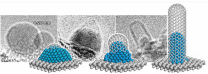
In collaboration with:
Prof. J. Robertson
References:
Wirth et al. Chem. Mater. 24, 4633 (2012)
Hofmann et al. Nano Lett. 7, 602 (2007)![]() In-situ metrology & Technology development
In-situ metrology & Technology development
We systematically develop and apply in-situ metrology to probe and understand the atomic level mechanisms that govern the growth and device behaviour of nanomaterials in realistic process environments. We thereby explore a wide range of techniques, incl. high-pressure XPS, in-situ XRD, environmental TEM and SEM, in-situ STM and in-situ optical spectroscopy. We aim at correlative probing at industrially relevant process conditions and explore additional degrees of freedom via MEMS type holder designs.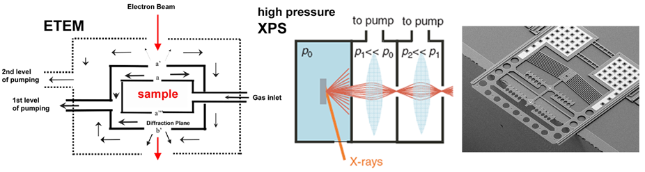
We recently developed and installed a near ambient pressure (NAP) X-ray photoemission spectroscopy (XPS) system is for high-throughput chemical surface analysis under application-relevant environmental conditions. This user facility is part of the Henry Royce Institute at Cambridge and please see the facility web page regarding access.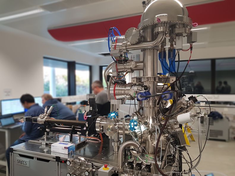
In collaboration with:
Dr F. Ross (IBM)
Prof. R. Schloegl (FHI, Germany)
Dr C. Cepek, Dr C. Africh (CNR, Italy)
Prof. J. Baumberg (Physics, University of Cambridge)
References:
Panciera et al. Nature Comm. 7, 12271 (2016)
Di Martino et al. Nano Lett. 15, 7452 (2015)
Weatherup et al. JACS 136, 13698 (2014)
Patera et al. ACS Nano 7, 7901 (2013)
CVD enabled 2D Material Technology and Devices
Future novel materials are unlikely to have high intrinsic value just by themselves. Instead it is the way that “new” and “old” materials will be integrated into components and systems to enable new designs and improved performance that will provide the value and long-term impact. We investigate not only growth, process and characterisation/standardisation techniques for novel 2D materials, but also address their effective interfacing with other “standard” materials and device and system integration across traditional boundaries. The challenge of interfacing 2D materials is quite different to bulk materials, as ultimately a 2D mono-layer has no “bulk” and intrinsic properties are hard to define as interface interactions can dictate their properties. Hence, more than ever, there is a need to understand interfacing and complex device behaviour of nanomaterials. We aim to address key questions of industrial materials development for 2D materials, including front and back end integration routes for a diverse set of near-term as well as future applications, ranging from advanced transparent conductors for organic light emitting diodes and liquid crystal devices, to opto-electronics, THz and lab-on-a-chip devices.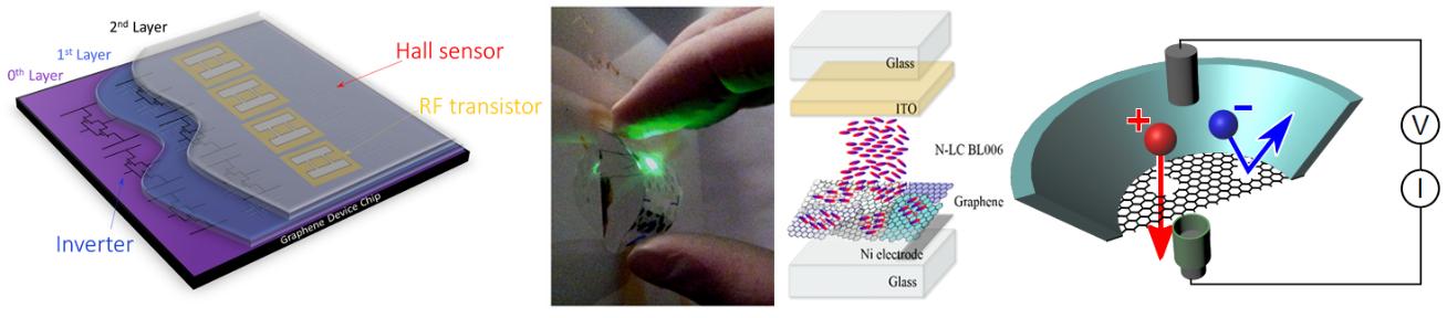
In collaboration with:
Prof. U. F. Keyser, Dr R. Degl’Innocenti, Prof. D. Ritchie (Physics, University of Cambridge)
Prof. T. Wilkinson, Prof. A. Nathan, Prof. J. M. Kim, Prof. J.Robertson, Prof. A. C. Ferrari (Engineering, University of Cambridge)
Thales (France)
Aixtron (UK)
Philips Centre for Process Innovation Ltd. (UK)
References:
Aria et al. ACS Appl. Mater. Interfaces 8, 30564 (2016)
Degl’Innocenti et al. ACS Photonics 3, 1747 (2016)
Walker et al. Appl. Phys. Lett. 107, 213104 (2015)
Qasim et al. Nanoscale 7, 14114 (2015)
Sanders et al. Nanoscale 7, 13135 (2015)
Advanced Materials for Energy Efficient Information and Communications Technologies (ICT) and Integrated Energy Systems
The field of ICT offers tremendous opportunity for radical technology changes, most of which will be driven by energy efficiency. Current technologies for energy usage, generation and storage all operate way below limits set by thermodynamics and there is huge potential to introduce radical changes that derive from fundamental scientific advances in materials-based technologies. The added value from improved energy efficiency is very high in the ICT sector, particularly for mobile devices. This makes the ICT sector one of the most attractive market entry points for new materials technologies. We investigate the use of nanostructured materials for instance in electrode materials and thermoelectric devices. We target a fully integrated approach, from the design and synthesis of new materials, their integration at the nano- meso- and micronscale into composite structures with controlled interfaces, and their integration into the device. The challenge is to control interfacial structures, both “as-synthesized/grown”, but more critically under the differing conditions of, for example, temperature and chemical potential occurring during operation. We use new metrologies to characterise interfaces under operando conditions, and via understanding the key underlying mechanisms aim at new design principles. In collaboration with:
Prof. C. Grey (Chemistry, University of Cambridge)
Prof. H. Sirringhaus (Physics, University of Cambridge)
Dr. R. V. Kumar (Materials, University of Cambridge)
Prof. R. Schloegl (FHI, Germany)
References:
Ogata et al. Nature Comm. 5, 3217 (2014)
Xi et al. Nanoscale 6, 5746 (2014)
Resistive Switching & Neuromorphic Computing
Resistive switches (RRAMs) are part of a range of emerging technologies that enable highly scalable non-volatile memory but also logic-in-memory architectures, i.e. bringing together logic and memory and thereby not only significantly increasing energy efficiency but also opening pathways to new functionality such as neuromorphics and cognitive computing. Towards this goal, we explore resistive switching phenomena in novel materials and device designs. We investigate new techniques to characterise in-operando the resistive switching effect in realistic device configurations, to foster an understanding of the nanoscale electrochemical reactions responsible for RRAM behaviour. In collaboration with:
Dr I. Valov (Peter Gruenberg Institute, Germany)
Prof. J. Driscoll (Materials, University of Cambridge)
Prof. J. Baumberg (Physics, University of Cambridge)
Dr G. Di Martino (Physics, University of Cambridge)
References:
Cho et al. Nature Comm. 7, 12373 (2016)
Di Martino et al. Small 12, 1334 (2015)
Spintronics
With hundreds of millions of computer hard drives sold every year, magnetism is currently the main repository of information storage. It is the electron “spin,” the elementary nanomagnet, that carries the information. Beyond storage, spintronics and such new device architectures are foreseen as the foundation for a new paradigm for information processing toward low power-consumption nonvolatile “green” electronics. We investigate new integrated electronic and spin-based device concepts based for instance on 2D materials. We also study the interfacing with chiral molecular semiconductor structures for spin engineered optoelectronic semiconductor devices.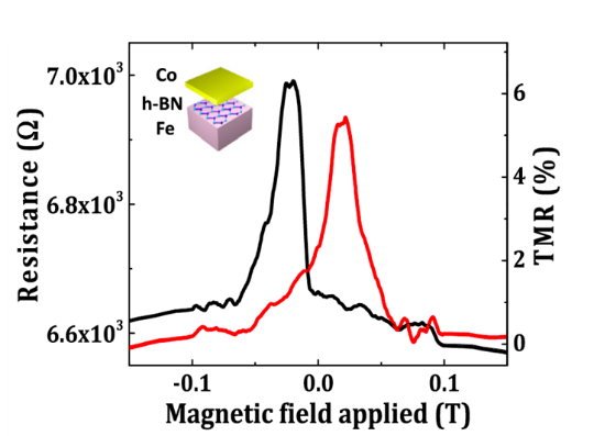 In collaboration with:
Prof P. Seneor, Prof. A. Fert (CNRS/Thales, France)
Prof. T. Endoh, Prof. K. Ito (Tohoku, Japan)
Prof. R. Friend (Physics, University of Cambridge)
Hitachi Cambridge Labs
References:
Piquemal-Bnaci et al. Appl. Phys. Lett. 108, 102404 (2016)
Dlubak et al. ACS Nano 6, 10930 (2012)
Biomimetics: functional dry adhesives
Non-specific dry adhesion, i.e. gluing on any surface without viscoelastic liquids or mating architectures such as hook-loop fasteners, is highly desirable for applications ranging from vacuum technology to robotics, space travel and medicine. The ability to control adhesion in nature is in many cases connected to van-der-Waals interactions and capillary forces on micro- and nanostructured contact surfaces. The feet of beetles, flies, spiders, and geckos are decorated with dense mats of hierarchical fibrillar structures enabling molecular contact over large areas, thus translating weak van-der-Waals interactions into enormous attractive forces which allow them to climb any wall. We are investigating new pathways to functional dry adhesives via hierarchically engineered structures, such as carbon nanotube-polymer structures. We systematically investigate the underlying adhesion mechanisms and are also interested in designing additional functional aspects, such as high electrical and thermal conductivity.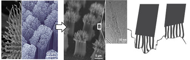 In collaboration with:
Dr. W. Federle (Zoology, University of Cambridge)
References:
Rong et al. Adv. Mat. 26, 1456 (2014)
Chen et al. ACS Appl. Mater. Interfaces 7, 3626 (2015)
Biosensor platform technology
We investigate novel, generic, real-time monitoring sensor technology, based on chemically modified graphene transducers. We currently focus on food allergen detection, as part of a feasibility study with industrial partners. We develop new 2D material-based device designs for large scale sensor integration.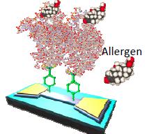 In collaboration with:
Prof. O. Guy (Swansea University)
National Physical Laboratory (NPL)
Unilever
Hexagonfab