| enginuity |
|
Flat screen research takes inspiration from a wee DRAM
Piero Migliorato is leading a team working with GEC Hirst Research Centre to develop large-area flat screen displays for applications, such as high definition TV. The large screens required for this application, in excess of 1300 x 900 pixels and a screen with a diagonal bigger than one metre, make cathode ray tubes unacceptable because of the size of tube required. Projection of the image formed on a liquid crystal display (LCD) is the best solution, but conventional LCD technology is not suitable to produce a TV image in terms of grey scale, colour and video. By using an active matrix however, this can be achieved. An active matrix LCD is one in which the switching of each pixel is controlled by a thin-film transistor deposited on to the inner surface of one of the glass substrates comprising the liquid crystal cell. Using this technology the screen is typically 2mm thick. At the back is an integrated circuit, containing an array of transistors forming each pixel. This is the same type of circuit used for a dynamic random access memory (DRAM), except that the circuit has to be fabricated on glass rather than on silicon, which means that lower temperatures have to be used in manufacturing.
Two materials are available for use as the channel material for these devices: amorphous silicon and polycrystalline silicon. Polycrystalline silicon has many advantages over the amorphous type. For instance the logic circuits required to switch the array of transistors can be directly fabricated on to the screen.
By investigating the electronic properties of the polycrystalline silicon and theoretical modelling of its behaviour, Dr Migliorato is developing the software required to design circuits based on polycrystalline Si transistors.
The situation in the field of large area microelectronics is similar to that in single crystal silicon technology in the 60s,' says Dr Migliorato. 'The polycrystalline material behaves differently because of the presence of large numbers of defects which change the band structure radically.'
A new type of circuit has been developed by Dr Migliorato's team, which consists of operational amplifiers. These operational amplifiers can be fabricated directly on to the glass used for the LCD cells and they increase the signal processing capability enormously. Applications include image sensors used for document scanning eg in fax machines, digital X-ray scanning for medical purposes, and a more speculative but important new application is in the fabrication of optically controlled neural networks (See the figure below).
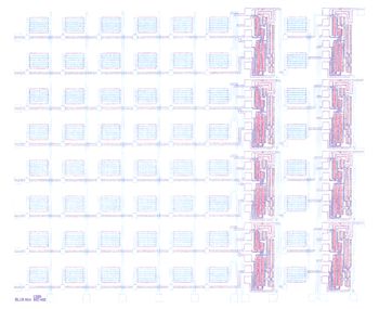
Circuit for a new type of neural network, developed in collaboration between Cambridge University Engineering Dept and GEC Hirst Research Centre within the framework of an SERCIDTI programme. The network consists of amorphous silicon photoresistors and polycrystalline silicon operational amplifiers.
| number 1, summer '93 |