|
|
||||||||

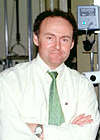
Professor Mark Welland
Mark Welland came to Cambridge in 1987 from a job with IBM in New York. While with IBM, he was involved in a major project to build a scanning tunneling microscope, and he still has one of the first photographs taken with it, showing the arrangement of silicon atoms on a surface. This was sufficiently exciting for him to want to set up a research group using such an instrument, as he could see there was tremendous scope.
With a colleague from Oxford, he arrived at the Engineering Department and set about getting funding to set up this facility in the UK at a time when no such thing existed. He is happy to report that since then over fifty research groups have been set up using this technology.
It was and is a big challenge, bridging the disciplines of physics and engineering, and Mark is hoping to see this link extended with the formation of a new interdisciplinary centre for nanotechnology, for which a bid is currently being formulated.
 "I
have always been interested in making things and understanding how they
work at a very fundamental level," he explains. "My work involves everything
from moving atoms about to making very delicate sensors for a variety
of applications. I try never to restrict myself in to one field of research
as I believe it is important to have ever-expanding interests. I am now
interested in developing biologically based devices, which is a new challenge.
I enjoy challenges."
With two children aged nine and twelve, and the first of 'another batch' on the way, Mark takes family life very seriously. "My children are more important to me than anything else."
He also keeps fit by running, playing squash and rowing for his college (St John's). Mark also enjoys reading, particularly on the philosophy of science and history. In common with many academics he travels a lot and always tries to find out as much as possible about the culture of the places he visits.