| enginuity |
|
Scanning Probe Microscopy
The ability to image and move individual atoms around is now a reality with the technique of Scanning Probe Microscopy. The Engineering Department's Scanning Electron Microprobe group, led by Dr Mark Welland, is the largest group operating in the UK. Scanning Probe Microscopy (SPM) is unique in that it will give real-time atomic images. A sharp point or probe is scanned over the surface to be analysed, and interactions between the probe tip and the surface are measured and used to provide information about that surface. An image is formed which is dependent on the interaction being measured.
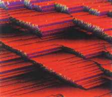
Heavily stepped region of the surface of Iron silicide.
Surface properties
The changes detected produce a contrast and thus a measure of the surface properties. By combining local property measurements such as electron, optical, magnetic, attractive and repulsive atomic forces with an atomic image, the topography related to a particular property can be determined.
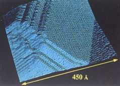
STM Image of Titanium Silicide - a material used In the microelectronics industry. The atomic structure of the TiSi2 is clearly visible.
There is also scope for atomic engineering. Dr Welland talks glibly about moving atoms around with the probe yet the problems in mechanically engineering a system capable of movements on an atomic scale are remarkable in themselves. Movement of atoms (for nano-fabrication) is possible because the strength of the interaction at the probe tip can allow individual atoms to be 'picked up'. Some examples of applications are shown in the accompanying photographs.
Mark Welland is currently co-ordinating a SERC initiative which has been funded at a level of £6M over five years to study various aspects of SPM.
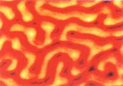
Magnetic force image of cobalt-palladium multilayer film showing magnetic domain structure. Image dimensions 4.3µm x 4.3µm.
Further information from Dr Mark Welland on (01223) 332676.
| number 2, spring '94 |