The Early History and Development of The Scanning Electron
Microscope
Bernie C Breton
The following information has been compiled from various
articles and my personal knowledge of many of the personalities involved.
When I began here in 1981, my lab was adjacent to Prof. Sir Charles
Oatley during his retirement years at the Engineering Labs. All but one of Oatley's students are still
very active to-day. Sadly, Ken Sander ( Oatley's first student on the electron
microscope) died some years ago.
The early history of the Scanning Electron Microscope
(SEM) is filled with many amusing stories. It was one of my great ambitions to write
the complete book one day .....and this has happened. The book was published by Academic Press Vol 133. This is a contribution by all of his research students and many others. However, one story that
the Prof. used to tell, is that when the SEM was being considered as a
commercial product, a group of Marketing experts were sent out to make
an evaluation of the number of SEMs that could be sold. Hang on to your
hat...they came back with... probably between 6 (six), and 10 (ten) would
saturate the market! Of course, they got it all wrong, the reason being
that they asked existing Electron Microscope users if they could use a
microscope that could, at that time, only do about 200 Angstroms resolution
(1 nm=10 Angstrom units). (The transmission electron microscope (TEM) was
at that time producing sub-50 Angstrom.) Today there are in excess of 50,000
SEMs world-wide. So much for marketing!
The earliest known work describing the concept of a Scanning
Electron Microscope was by M. Knoll (1935) who, along with other pioneers
in the field of electron optics, was working in Germany. Subsequently M.
von Ardenne (1938) constructed a scanning transmission electron microscope
(STEM) by adding scan coils to a transmission electron microscope. The
first STEM micrograph was of a ZnO crystal imaged at an operating voltage
of 23 kV at a magnification of 8000 times, and a spatial resolution between
50 and 100 nm. The micrograph contained 400 x 400 scan lines and took 20
min to record, because the film was mechanically scanned in synch
with the beam. The instrument had two electrostatic lenses, with the scan
coils placed between them. The instrument also had a viewing CRT, but it
was not used to record the image
The first SEM used to examine the surface of a solid specimen
was described by Zworykin et al. (1942), working in the RCA Laboratories
in the United States. The electron optics of the instrument consisted of
three electrostatic lenses with scan coils placed between the second and
third lenses The electron gun was located at the bottom so the specimen
chamber was at a comfortable height for the operator. This was a common
practice in the early days. It did suffer from the slight problem however,
that the specimen might fall down the column. A resolution of about 50
nm was achieved with this first SEM. By comparison with the rapidly developing
TEM, this figure was considered unexciting and further development lapsed.
In the late 1940s C. W. Oatley, then a lecturer in the
Engineering Department of Cambridge University, England, became interested
in conducting research in the field of electron optics and decided to re-investigate
the SEM as a complement to the work being done on the TEM by V. E. Cosslett,
also in Cambridge at the Physics Department. One of Oatley's students,
Ken Sander, began work on a column for a transmission electron microscope
using electrostatic lenses, but Ken took ill after about one year and had
to leave for a time. This work then was taken up by Dennis McMullan in
1948, and he and Oatley built their first SEM. By 1952 this instrument
had achieved a resolution of 50 nm, but by far the most important thing
about this SEM is that it produced the first micrographs showing the striking
three-dimensional imaging characteristics of the modern-day SEM (McMullan
(1953)).
Dennis McMullan was followed by Ken
Smith (started 1952) who took over SEM1, made a number of improvements to
the electron optical system, and improved the efficiency of secondary electron
collection. He showed for the first time that a stable image could be formed
using the true low-energy component of the total secondary emission. Ken has
told me personally that during this period in the development of the SEM, microscopists
in general showed virtually no interest in the instrument, and he and Oatley
were continually looking for applications to promote the SEM; many which they
tried were never published. However, they published the first paper setting
out clearly the fields of application for the SEM (Smith and Oatley (1955)).
The third research student on the SEM under Oatley's supervision was O. C.
Wells (started 1953), who built a second SEM, also incorporating electrostatic
lenses; unlike SEM1, however, this instrument had the gun at the bottom of the
column - a configuration considered better for experimental work. All SEMs built
in the Engineering Department subsequently conformed to this layout. Wells pioneered
the use of the scintillator backscattered (BSE) detector (as an alternative
to the secondary electron multiplier used in SEM1) and applied his SEM to many
new types of specimen including a large-scale study of fibres. He was also the
first to use stereographic pairs to produce SEM micrographs with quantifiable
depth information (Wells (1960)).
The next important step was taken by Oatley's fourth research
student, Everhart (started 1955), who improved the secondary electron (SE)
detector by using a scintillator to convert electrons to photons, which
were then transmitted by a light pipe directly interfaced to the photomultiplier
tube. This idea was followed up by Thornley (started 1957), and their ground-breaking
work resulted in the publication of a much-quoted paper: "Wide-band detector
for micro-microampere low-energy electron currents" (Everhart and Thornley
(1960)). Replacement of the electron multiplier with the new scintillator/photomultiplier
combination increased the amount of signal collected and resulted in an
improvement in signal-to-noise ratio. Hence, weak contrast mechanisms,
such as voltage contrast (discovered by Oatley and Everhart (1957)) could
be better investigated. The term " voltage contrast" evolved from the fact
that as the voltage applied to a specimen was changed, the image contrast
changed. (Tom Everhart and Oatley were investigating this one day and Tom
said: " Well, voltage contrast!" and the term has stuck to this day). Image
interpretation was also improved in this early period of research when
both Everhart and Wells made the first quantitative studies of the effects
of beam penetration on image formation in the SEM.
It was always one of Oatley's great ambitions to produce
and market a really simple low-cost SEM; he argued that most of
the work undertaken by microscopists did not require high resolution. To
further this idea Peter Spreadbury, his fifth student (started 1956), built
a simple SEM utilising a CRT as a display unit.
New fields of application were opened up by Gary Stewart
(started 1958) who fitted an ion gun to the SEM specimen chamber to allow
ion bombardment of the specimen. After his research, Gary went on to the
Cambridge Instrument Company to pioneer the production of the Stereoscan.
The ion beam work was later extended by Alec Broers (started 1961) who
improved the ion beam optics of the instrument and added a magnetic objective
lens to improve resolution. He used this set-up to conduct some of the
earliest experiments in electron beam microfabrication. Another breakthrough
was achieved by Haroon Ahmed (started 1959) who modified the SEM built
by Wells (SEM2) to enable the examination of thermionic emitters at temperatures
exceeding 1000K. The first SEM in the Department to achieve a resolution
of 10 nm was built by Fabian Pease (started 1960). This was an all magnetic
lens SEM, the fifth to be constructed in the Group. Several of these SEMs
were later manufactured in the Departmental Workshops and used by other
Groups within the University.
No description of the work in Oatley's Group would be
complete without mention of Les Peters, chief technician, who had a hand
in the construction of all the instruments described and helped all the
research students with their experimental work. For his services to the
Department Les was awarded an honorary MA degree by the University in 1990.
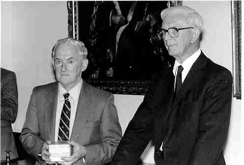
Pictured here are Les Peters and Charles Oatley together in the Board Room
of the Engineering Department on the occasion of a celebration held to
mark the event. The contribution of Joan Duffield, Charles Oatley's secretary, to the success of this early work must also be recognised. She organised all the paperwork
for the Group, typed the technical papers and typed the majority of the research students' dissertations - in the days when five all-correct carbon copies were the norm and word processors were unheard of! Her work in those early days
was invaluable.
With his appointment in 1960 to the Chair of Electrical Engineering in the
Department, Charles Oatley's direct involvement in the supervision of research
students came to an end; this task was taken over by Bill Nixon who joined the
Group in 1959 having worked in the Cavendish EM Group with V. E. Cosslett for
a number of years. So ended the first phase of the research on the scanning
electron microscope at the University Engineering Department.
References and acknowledgements;
I would like to thank KCA Smith for the his encouragement, contributions and support in generating this information. A paper present by Ken at EMAG 97 is reprinted here with kind permission of the IOP. Much of this information and a great deal more was published in our book.
Everhart TE, Thornley RFM (1960): Wide-band detector for
micro-microampere low-energy electron currents. J. Sci. Instrum. 37, 246-248
.
Knoll M (1935): Aufladepotentiel und Sekundäremission
elektronenbestrahlter Körper. Z tech. Phys. 16, 467-475
McMullan D (1953): An improved scanning electron microscope
for opaque specimens; Proc. Inst. Electr. Engrs 100, Part II, 245-249.
Reprinted in: Selected Papers in Electron optics, Vol. MS94 (Ed. Hawkes
PW). SPIE milestones (1994) 186-200
Oatley CW and Everhart TE (1957): The examination of p-n
junctions in the scanning electron microscope. J. Electronics 2, 568-570.
Smith KCA and Oatley CW (1955): The scanning electron
microscope and its fields of application. Br. J. Appl. Phys. 6, 391-399.
von Ardenne M (1938a): Das Elektronen-Rastermikroskop.
Theoretische Grundlagen. Z. Phys. 109, 553-572.
von Ardenne M (1938b): Das Elektronen-Rastermikroskop.
Praktische Ausführung. Z. tech. Phys. 19, 407-416
Wells OC (1960): Correction of errors in electron stereomicroscopy.
Br. J. Appl. Phys. 11, 119-201.
Zworykin VA, Hillier J and Snyder RL (1942): A scanning
electron microscope. ASTM Bull. 117, 15-23.